KiCad is a popular open-source software suite used for electronic design automation (EDA). One of the primary features of KiCad is its ability to design two-layer printed circuit boards (PCBs). PCBs are essential components of electronic devices, providing a platform for the components to be mounted and connected.
Designing a two-layer PCB with KiCad involves creating a schematic diagram, defining the board outline, placing components, routing traces, and generating manufacturing files. KiCad’s user-friendly interface and extensive library of components make it an accessible tool for hobbyists and professionals alike. With KiCad, users can create custom PCBs for a variety of applications, from simple LED circuits to complex microcontroller designs.

Overview
What is KiCad 2 Layer PCB?
KiCad is a free, open-source software suite for electronic design automation (EDA) that allows users to design schematics and printed circuit boards (PCBs). KiCad 2 Layer PCB is a type of PCB that is designed using KiCad software and consists of two layers of copper traces separated by a layer of insulating material.
Benefits of KiCad 2 Layer PCB
KiCad 2 Layer PCB has several advantages over other types of PCBs:
- Affordability: KiCad is a free software, which means that designing KiCad 2 Layer PCBs is significantly cheaper than using proprietary software.
- Ease of Use: KiCad is user-friendly and easy to learn, making it accessible to both hobbyists and professionals.
- Flexibility: KiCad allows users to customize their designs to meet specific requirements, making it a versatile option for various applications.
- Reliability: KiCad 2 Layer PCBs are reliable and durable, making them ideal for use in high-performance applications.
- Compatibility: KiCad is compatible with various operating systems, including Windows, Linux, and macOS.
KiCad 2 Layer PCB is an excellent option for those looking to design a reliable, affordable, and customizable PCB.
Designing KiCad 2 Layer PCB
Schematic Capture
Schematic capture is the first step in designing a KiCad 2 Layer PCB. It involves creating a visual representation of the circuit using schematic symbols. The schematic capture tool in KiCad is user-friendly and intuitive, making it easy to drag and drop components and connect them with wires.
When creating the schematic, it is important to pay attention to the net names. Net names are used to connect components on the schematic to the corresponding pads on the PCB layout. It is also important to add any necessary labels and annotations to the schematic for clarity.
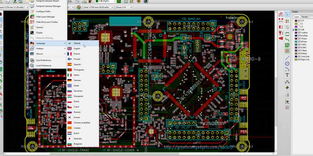
PCB Layout
Once the schematic is complete, the next step is to create the PCB layout. The PCB layout tool in KiCad allows users to place components on the board, route traces between them, and add any necessary copper pours or planes.
When designing a 2 layer PCB, it is important to keep in mind the limitations of the two layers. Components should be placed in a way that allows for easy routing of traces and minimizes the need for vias. The placement of decoupling capacitors and power supply components is also important for minimizing noise and ensuring proper power delivery.
Netlist Generation
After the PCB layout is complete, the next step is to generate the netlist. The netlist is a file that contains information about the connections between components on the PCB layout. It is used by the PCB manufacturing software to generate the final PCB.
In KiCad, the netlist can be generated by running the “ERC” (electrical rule check) and “DRC” (design rule check) tools. These tools ensure that the PCB design is electrically and mechanically sound before generating the netlist.
Overall, designing a KiCad 2 Layer PCB involves creating a schematic, laying out the components on the PCB, and generating a netlist. With the user-friendly tools and intuitive interface of KiCad, designing a 2 layer PCB can be a straightforward process.
Manufacturing KiCad 2 Layer PCB

Exporting Gerber Files
Before you can manufacture a KiCad 2 layer PCB, you need to export the Gerber files. These files contain all the necessary information for the manufacturer to create the PCB. To export the Gerber files, go to File > Plot in KiCad and select the layers you want to export. Make sure to select the correct units and format for your manufacturer.
Drilling and Milling
Once you have the Gerber files, the manufacturer will drill and mill the PCB. The manufacturer will use the drill files to create the holes in the PCB and the milling files to cut the PCB to the correct size and shape. Make sure to specify the correct drill sizes and tolerances for your design.
Solder Mask
The solder mask is a layer of material that is applied to the PCB to protect the copper traces from oxidation and to prevent solder from flowing where it shouldn’t. To add a solder mask to your KiCad 2 layer PCB, you will need to export the solder mask Gerber file. Make sure to specify the correct color and thickness for your design.
Silk Screen
The silk screen is a layer of text and graphics that is printed on top of the PCB to indicate component placement and polarity. To add a silk screen to your KiCad 2 layer PCB, you will need to export the silk screen Gerber file. Make sure to specify the correct color and font for your design.
That’s it! With these steps, you can manufacture a KiCad 2 layer PCB.
Troubleshooting KiCad 2 Layer PCB
Common Issues and Solutions
When designing a KiCad 2 layer PCB, it is common to encounter issues that can affect the functionality of the board. Here are some of the most common issues and their solutions:
Issue: Incorrect Netlist
One of the most common issues that designers face is an incorrect netlist. This can happen when the schematic and the PCB layout do not match. To solve this issue, the designer needs to make sure that the schematic and the PCB layout are synchronized. This can be done by using the “Update PCB from Schematic” tool in KiCad.
Issue: Missing Connections
Another common issue is missing connections. This can happen when the designer forgets to connect a component to the rest of the circuit. To solve this issue, the designer needs to go back to the schematic and make sure that all the connections are properly made.
Issue: Incorrect Footprints
Sometimes, the designer may use the wrong footprint for a component. This can cause issues with the alignment of the component on the PCB. To solve this issue, the designer needs to make sure that the correct footprint is used for each component.
Issue: Short Circuits
Short circuits can occur when two or more nets are connected unintentionally. This can be caused by overlapping traces or components. To solve this issue, the designer needs to check the PCB layout for any overlapping traces or components and adjust them accordingly.
Issue: Unconnected Pins
Unconnected pins can cause issues with the functionality of the circuit. To solve this issue, the designer needs to make sure that all the pins of each component are properly connected to the rest of the circuit.
In conclusion, troubleshooting KiCad 2 layer PCBs can be a challenging task, but by following these common solutions, designers can ensure that their boards function properly.
