Table of Contents
ToggleKiCad is an open-source software suite that is used for electronic design automation (EDA). It is a popular tool for designing printed circuit boards (PCBs) and is widely used by hobbyists, students, and professionals alike. KiCad is known for its user-friendly interface and its ability to handle complex designs with ease.
One of the most attractive features of KiCad is that it is free and open-source. This means that anyone can use it without having to pay any licensing fees, and the source code is available for anyone to modify and improve. KiCad is also available on multiple platforms, including Windows, Linux, and macOS, making it accessible to a wide range of users.
KiCad is a powerful tool that can be used to create simple circuits as well as complex designs. It offers a range of features, including schematic capture, PCB layout, and 3D visualization. With KiCad, users can design circuits, create schematics, and lay out PCBs all in one integrated environment.

Getting Started
Installing KiCad
Before getting started with KiCad, you need to download and install the software. KiCad is available for Windows, Mac, and Linux. You can download the latest version of KiCad from the official website. Once the download is complete, follow the installation instructions to install the software on your computer.
Creating a New Project
After installing KiCad, you can start creating your first project. To create a new project, open KiCad and click on “File” in the top-left corner of the screen. From the drop-down menu, select “New Project.”
In the “Create New Project” window, enter a name for your project and select a location to save it. You can also choose a template for your project, such as a schematic or a PCB layout. Once you have entered all the required information, click on “OK” to create your new project.
Now that you have created a new project, you can start adding components to your schematic and designing your circuit. KiCad offers a wide range of tools and features to help you design your circuit, including a schematic editor, a PCB layout editor, and a 3D viewer.
In summary, getting started with KiCad is easy. First, download and install the software on your computer. Then, create a new project and start designing your circuit. With KiCad’s powerful tools and features, you can create simple and complex circuits with ease.
Designing the Simple Circuit

Adding Components
To design a simple circuit in KiCad, you first need to add components to your schematic. To do this, go to the “Add Component” button on the toolbar and select the component you want to add. Once you have selected your component, you can place it on the schematic by clicking on the location where you want it to go.
To make sure that your schematic is organized and easy to read, it’s a good idea to group your components by their function. You can also use the “Net Label” tool to label your components and connect them to each other.
Connecting Components
After you have added all the necessary components to your schematic, it’s time to connect them together. To do this, use the “Wire” tool to draw connections between the pins of your components. Make sure that your connections are clear and easy to follow.
If you need to cross wires without connecting them, you can use the “No Connect” symbol. This symbol is used to indicate that two wires should not be connected to each other.
Once you have connected all your components, you can use the “Generate Netlist” tool to create a list of all the connections in your schematic. This list can then be used to create a PCB layout for your circuit.
Overall, designing a simple circuit in KiCad is a straightforward process that requires a basic understanding of electronics and some patience. With practice, you can create complex circuits with ease using this powerful software.
Schematic Capture

Creating a Schematic
KiCad is a popular open-source software tool for designing electronic circuits. The schematic capture feature in KiCad allows users to create a graphical representation of a circuit. This is an important step in the design process as it helps users to visualize the components and connections in the circuit.
To create a schematic in KiCad, users can start by opening the Eeschema application. From there, they can create a new project and start adding components to the schematic. The software provides a library of components that users can choose from, or they can create their own custom components.
Once the components are added to the schematic, users can start connecting them by adding wires. The software provides a range of tools to help users create and modify wires, including the ability to add bends, move endpoints, and adjust the routing style.
Checking for Errors
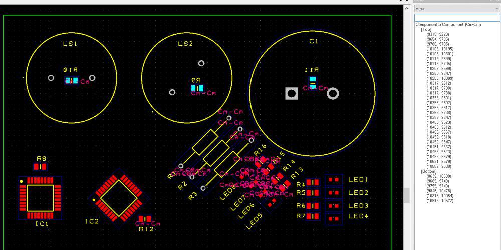
After creating the schematic, it’s important to check for errors before moving on to the next stage of the design process. KiCad provides a range of tools to help users check for errors, including the Electrical Rules Check (ERC) and the Design Rule Check (DRC).
The ERC is used to check the schematic for electrical errors, such as missing connections or incorrect pin assignments. The DRC is used to check the schematic against a set of design rules, such as minimum trace width or clearance between components.
Users can customize the design rules to match their specific requirements, and the software will highlight any violations so that they can be corrected. Once all errors have been resolved, the schematic is ready to be used in the next stage of the design process.
In conclusion, the schematic capture feature in KiCad is an essential tool for designing electronic circuits. By following the steps outlined in this section, users can create a clear and accurate representation of their circuit, and ensure that it is error-free before moving on to the next stage of the design process.
PCB Layout

Transferring the Schematic to the PCB
Once you have completed the schematic, the next step is to transfer it to the PCB layout. This process involves creating a physical representation of the circuit board that you will be manufacturing. KiCad has a built-in tool that allows you to transfer the schematic to the PCB layout with ease.
Placing Components
After transferring the schematic to the PCB layout, the next step is to place the components. It is important to consider the placement of the components as this can affect the functionality of the circuit. KiCad provides a variety of tools to help you place components accurately. You can use the grid and snap tools to align the components and ensure that they are placed correctly.
Routing the PCB
The final step in creating a PCB layout is routing the PCB. This involves creating connections between the components on the board. KiCad provides a range of tools to help you route the PCB efficiently. You can use the auto-router tool to automatically create connections between the components. Alternatively, you can use the manual routing tool to create connections manually.
Overall, KiCad provides a simple and efficient way to create a PCB layout. By following the steps outlined above, you can create a high-quality PCB layout that is both functional and aesthetically pleasing.
Manufacturing

Generating Gerber Files
Once your circuit design is complete, you can generate Gerber files using KiCAD’s built-in tools. Gerber files are a standard format used by PCB manufacturers to create the physical board. To generate Gerber files, simply go to the “Plot” menu and select the layers you want to include in the output. You can also customize the output settings, such as the resolution and format of the files.
Ordering PCBs
Once you have your Gerber files, you can send them to a PCB manufacturer to have the physical board made. There are many PCB manufacturers to choose from, and prices and lead times can vary widely. Some popular options include JLCPCB, PCBWay, and OSH Park.
When ordering PCBs, it’s important to double-check your design and specifications to ensure that the manufacturer can produce the board correctly. This includes checking the board size, hole sizes, and placement of components. You should also consider the type of board material and thickness, as well as any special requirements such as gold plating or surface finish.
Overall, the process of manufacturing a simple circuit using KiCAD is straightforward and accessible to beginners. With the right tools and resources, anyone can create a custom PCB for their project.

