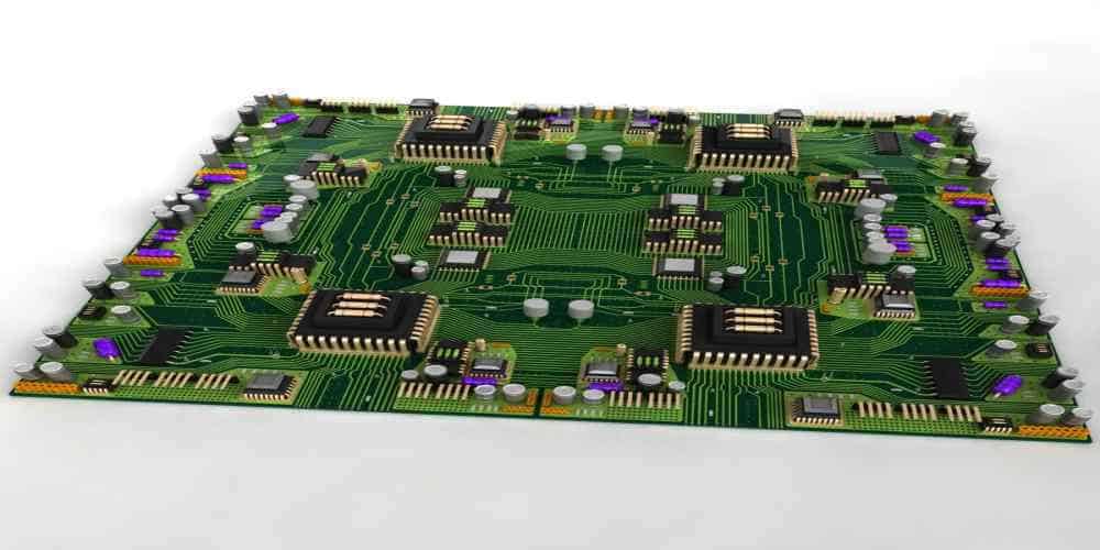
What is a large circuit board?
A PCB (Printed Circuit Board) that is physically bigger than a standard-size board is called a huge circuit board. Generally, a circuit board is big if it surpasses a standard-size PCB. However, the size might vary based on the application and design needs.
The design, price, and functioning of a PCB can all depend on its size. For example, oversized circuit boards could need more layers, routing, and expensive materials. They also need specialized production techniques or tools to accommodate their size and complexity.
Large circuit boards are frequently employed when additional surface area or component space is needed. These can include systems that require a lot of components. Examples include telecommunications or industrial control systems, or systems that demand considerable power, such as power supply or motor controllers.
Large circuit board design and production demand particular skills and understanding. For example, engineers and designers must carefully consider signal integrity, thermal management, and manufacturing tolerances to ensure the board performs as intended and adheres to the requirements.
Working closely with a reputable and knowledgeable PCB maker that can offer direction and help throughout the process is crucial when designing a big circuit board. The manufacturer can offer assistance with designing for manufacture. Additionally, they can suggest suitable materials and production methods. They can also offer testing and inspection services to guarantee that the board satisfies the requirements. Engineers and designers may ensure their big circuit board design is successful and satisfies their application’s requirements by collaborating closely with a reliable PCB manufacturer.
Creating the Circuitry Design
Large PCB (Printed Circuit Board) circuitry design involves careful planning and considering the project’s unique requirements. We must create a schematic diagram, lay out the PCB, verify, and generate fabrication and Gerber files to manage the PCB manufacturing process. These are essential procedures to do. Using these measures, you can ensure that the PCB has enough room for routing, thermal management, and all the required components.
Circuit Board Layering
An essential component of massive PCB design and manufacture is circuit board stacking. It impacts manufacturing costs, heat management, signal integrity, and electrical performance. The impedance, capacitance, and inductance of the traces and connections can depend on the thickness and spacing of the copper layers, which can impact signal quality and overall circuit performance. In addition, signal integrity, which is essential for high-speed digital and analog circuits, can be impacted by layering. Therefore, the layer stackup should guarantee the electrical performance satisfies the project’s needs.
Electrical performance, signal integrity, thermal management, and manufacturing cost criteria are all impacted by circuit board stacking. It makes it a crucial component of big PCB design and manufacture. However, these problems may reduce, and a proper layer stackup design can guarantee that the PCB satisfies the necessary signal integrity requirements.
Drilling Holes
Large PCBs must go through a crucial process called drilling holes to attach components and create connections between the board’s many layers. To guarantee the optimization of the drilling process for the project’s particular requirements, it is essential to consider the holes’ size and depth, location, the drilling technique, quality control, and working with an experienced PCB maker. In addition, we should consider the size and positioning of the holes as well as the drilling process itself.
Silk-Screening
The top layer of a PCB, the silk screen, is a reference guide for positioning components on the board. Therefore, it needs a specially designed ink that comes in various colors but is often white. It may also be red, black, yellow, or blue. The PCB board’s valuable information, such as component values, part numbers, test locations, and polarity, is specified on the silk screen to help/assist users during assembly. Liquid photo imaging (LPI), manual screen printing, and direct legend printing are the primary techniques for adding a silk-screen coating to a PCB (DLP). Although it is the most exact method, adding a silk-screen is highly costly.
Bare-board test
Before putting components like ICs on a bare circuit board, you verify the isolation and continuity of the electrical connections. This is known as “bare board testing.” It requires ensuring no open spots in the circuit and that the requisite resistance between two electrical connections is satisfied. We conduct these tests with a threshold between 10 and 50 ohms and under 100 milliamps.
The “bed of nails” tester and the “flying probe tester” are the two primary categories of bare board test devices. A special contraption called the bed of nails tester holds the PCB in place while testing it using a unique set of spring-loaded pogo pins. The flying probe tester uses two or more “flying probes” to glide across the board’s surface and test each net without needing a special fixture for the circuit. Unfortunately, it needs a significant financial investment, a new fixture, and an array of pogo pins for each PCB, which makes it slower and less adaptable.
Assembly
To guarantee that the constructed PCB is functioning and that there are no problems with the components or soldering, quality control is required. Testing is a crucial phase throughout the assembly process that may need specific tools and methods. Partnering with a knowledgeable PCB maker can assist in optimizing the assembly procedure for the project’s unique requirements.
Challenges of designing large circuit boards

Fabricating large PCBs presents several challenges due to their size and complexity. Overall, fabricating large PCBs presents several challenges we must address to ensure that the PCB is high quality and meets the project’s requirements. Here are some of the main challenges associated with fabricating large PCBs:
Switching regulators with an incorrect layout
Although linear voltage regulators are less expensive than traditional ones, switching regulators are more efficient. However, while using it effectively, linear voltage regulators utilize a significant amount of electricity, which causes considerable heat dissipation.
Misaligned Design and Drawing
Significant errors in a PCB’s final design process might result from comparative disparities in Design & Drafting. Therefore, compare the dimensions of the drawing to the data, number of holes, size of the pad, and revision levels. The lesson here is to check your designs against the original schematic constantly.
Acid Traps
Acid traps happen when two traces intersect at an extremely sharp angle. It increases the likelihood that the etching solution used to remove copper from the blank board may become stuck or trapped. As a result, traces lose connection with the allocated nets and become open-circuited. By switching to light-triggered etching solutions in recent years, fabricators have lessened the problem of acid traps.
Components’ Tombstoning
Little passive SMT electronic components tend to lift on one end and “tombstone” when soldered to a PCB assembly using a reflow process. Incorrect landing techniques and an imbalance in the thermal relief provided to the device’s pads are frequently the causes of tombstoning.
Lack of Wide High Power Traces
The minimum PCB trace width threshold won’t be enough if the PCB Board traces must carry currents larger than 500mA. An inside trace can carry less information than one on an exterior layer at a given thickness. The exterior trace has better ventilation and thermal dissipation, which explains this. How much copper is ideal for that layer determines the breadth. Most PCB manufacturers provide copper weight options, ranging from 0.5 oz/sq.ft to 2.5 oz/sq.ft.
