Altium is a software tool that has been widely used for designing printed circuit boards (PCBs) for many years. The layout of a PCB is a crucial aspect of its design, and Altium provides a range of features to help engineers create high-quality layouts efficiently.
One of the key benefits of using Altium is that it offers a user-friendly interface that allows engineers to quickly and easily create PCB layouts. The software provides a range of tools and features that can help engineers to optimize their PCB designs, including the ability to create custom components, import and export design files, and collaborate with other team members.
Overall, Altium is a powerful tool that can help engineers to create high-quality PCB layouts quickly and efficiently. By providing a range of features and tools, Altium makes it easy for engineers to optimize their designs and collaborate with other team members, making it an essential tool for any PCB design project.
Basics of Layout in Altium
Creating a New Layout
When you first open Altium, you will be prompted to create a new project. From there, you can create a new PCB layout by selecting “File” > “New” > “PCB” from the menu bar. Alternatively, you can create a new layout from an existing schematic by selecting “Design” > “Import Changes from PCB” from the schematic editor.
Once you have created a new layout, you will need to set up the workspace to begin designing your PCB.
Setting Up the Workspace
The workspace in Altium is divided into several panels, including the “Navigator,” “Properties,” and “PCB” panels. These panels can be customized to suit your needs by selecting “View” > “Panels” from the menu bar.
To begin designing your PCB, you will need to add components to the layout. You can do this by selecting “Place” > “Component” from the menu bar and selecting the desired component from the library browser. Once you have placed the component, you can move and rotate it as necessary using the “Move” and “Rotate” tools.
To connect the components, you will need to add traces between them. You can do this by selecting “Place” > “Track” from the menu bar and clicking on the starting point for the trace. You can then drag the trace to the desired endpoint and adjust its properties using the “Properties” panel.
Overall, Altium provides a comprehensive set of tools for designing PCB layouts. By following these basic steps, you can begin creating your own layouts with ease.
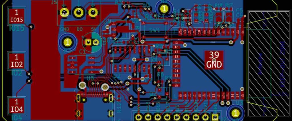
Designing the Board
Placing Components
The first step in designing a PCB layout is to place the components on the board. It’s important to take into account the size and shape of each component, as well as their orientation and spacing. Altium provides a variety of tools to help with this process, including the ability to snap components to a grid and align them with other components.
When placing components, it’s also important to consider the signal flow and the location of connectors and ports. This can help to minimize trace lengths and reduce the risk of signal interference.
Routing Traces
Once the components have been placed, the next step is to route the traces that connect them. Altium provides a range of tools to help with this process, including automatic routing and interactive routing.
When routing traces, it’s important to consider factors such as signal integrity, power distribution, and thermal management. This can involve using different trace widths and layer configurations, as well as adding vias to connect traces between different layers.
Adding Vias
Vias are a critical component of any PCB layout, as they provide a way to connect traces between different layers of the board. Altium provides a range of tools to help with via placement, including the ability to automatically add vias based on design rules.
When adding vias, it’s important to consider factors such as signal integrity, thermal management, and manufacturability. This can involve using different via sizes and configurations, as well as optimizing the placement of vias to minimize signal interference and ensure reliable operation.
Overall, designing a PCB layout in Altium requires careful consideration of a range of factors, from component placement and trace routing to via placement and signal integrity. With the right tools and techniques, however, it’s possible to create a high-quality layout that meets the needs of your project.
Advanced Techniques

Using Copper Pour
Copper Pour is a powerful tool in Altium that allows you to create large areas of copper on your PCB layout. This feature can be used to create a ground plane or power plane, which can help improve the performance of your board. To use Copper Pour, select the polygon tool and draw a shape that covers the area you want to fill with copper. Then, right-click on the shape and select “Properties.” In the “Polygon Pour Properties” dialog box, you can adjust the settings for the Copper Pour, such as the net name and clearance.
Adding Fills
Fills are another useful feature in Altium that can help improve the performance of your board. Fills are used to create a solid area of copper on your PCB layout, which can help reduce the amount of noise and interference on your board. To add a fill, select the “Place Fill” tool and draw a shape that covers the area you want to fill. Then, right-click on the shape and select “Properties.” In the “Fill Properties” dialog box, you can adjust the settings for the fill, such as the net name and clearance.
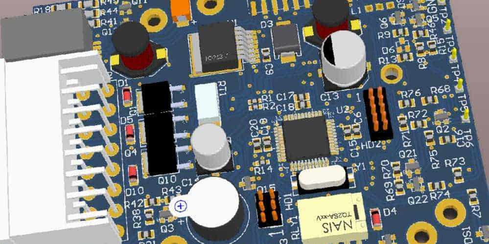
Creating Multi-Layer Boards
Multi-layer boards are becoming increasingly popular in the electronics industry, as they allow for more complex designs and smaller form factors. Altium provides a powerful set of tools for creating multi-layer boards, including the ability to add vias, planes, and routing layers. To create a multi-layer board, start by selecting the “Layer Stack Manager” from the “Design” menu. In the “Layer Stack Manager” dialog box, you can add and remove layers, adjust the thickness of each layer, and define the properties for each layer.
In conclusion, Altium provides a powerful set of tools for creating advanced PCB layouts. By using Copper Pour, Fills, and Multi-Layer Boards, you can create high-performance designs that meet the needs of your project.
Design Rules and Constraints
Setting Up Rules and Constraints
In Altium, design rules and constraints are used to ensure that the design meets specific requirements. These rules can be set up for various design aspects, such as clearance, trace width, and via size. Setting up rules and constraints is a crucial step in the design process, as it helps prevent errors and ensures that the design meets the required specifications.
To set up rules and constraints in Altium, go to the Design menu and select Rules. This will open the PCB Rules and Constraints Editor, where you can create and manage design rules. You can create new rules by clicking on the Add Rule button and selecting the type of rule you want to create.
Once you have created a rule, you can specify its parameters, such as the minimum and maximum values for clearance or trace width. You can also assign the rule to specific objects, such as nets or components, to ensure that it only applies to the desired design elements.
Checking for Errors
After setting up rules and constraints, it is essential to check the design for any errors. Altium provides various tools to help you check your design, such as the Design Rule Check (DRC) feature. The DRC checks the design against the rules and constraints you have set up and highlights any violations.
To run a DRC in Altium, go to the Tools menu and select Design Rule Check. This will open the Design Rule Check panel, where you can select the rules you want to check and run the DRC. Any violations will be highlighted in the PCB editor, and you can use the PCB Inspector panel to view the details of the violation and make the necessary changes.
In addition to the DRC, Altium also provides other tools, such as the Net Connectivity Check and the Clearance Matrix, to help you check your design for errors and ensure that it meets the required specifications.
Overall, setting up rules and constraints and checking the design for errors are crucial steps in the design process. By following these steps, you can ensure that your design meets the required specifications and prevent errors that could lead to costly mistakes.
Output and Manufacturing
Generating Gerber Files
Gerber files are essential to the manufacturing process, as they provide a standardized format for the various layers of a PCB design. To generate Gerber files in Altium, navigate to the “Fabrication Outputs” tab in the “Output Job” window. Here, you can select which layers to include in the Gerber files, as well as specify the file format and naming convention. It is important to double-check the settings before generating the files to ensure that they match the manufacturer’s requirements.
Creating Drill Files
Drill files are another crucial component of the manufacturing process, as they provide the necessary information for drilling holes in the PCB. In Altium, drill files can be generated in the same “Fabrication Outputs” tab as the Gerber files. Here, you can select the drill file format and specify the naming convention. Be sure to verify that the drill file settings match the manufacturer’s requirements before generating the files.
Exporting the Bill of Materials (BOM)
The Bill of Materials (BOM) is a list of all the components used in a PCB design, including their part numbers, quantities, and other relevant information. In Altium, the BOM can be exported in various formats, such as CSV or Excel. To export the BOM, navigate to the “Reports” tab in the “Output Job” window. Here, you can select the BOM format and specify the naming convention. It is important to review the BOM before exporting it to ensure that it is accurate and complete.
In conclusion, generating Gerber files, creating drill files, and exporting the BOM are crucial steps in the manufacturing process of a PCB design. Altium provides a user-friendly interface for performing these tasks, but it is important to verify that the settings match the manufacturer’s requirements to ensure a successful manufacturing process.
