PCI Express (PCIe) is a widely used interface for connecting peripherals to computer systems. PCIe is a high-speed serial interface that provides a high-bandwidth, low-latency communication channel between devices. PCIe is used in a variety of applications, including graphics cards, storage devices, and network adapters.
Designing a PCIe printed circuit board (PCB) is a complex process that requires careful consideration of many factors. A well-designed PCIe PCB can help ensure reliable operation of the system and improve performance. Some of the key factors to consider when designing a PCIe PCB include signal integrity, power management, and mechanical design. By paying close attention to these factors, designers can create a PCIe PCB that meets the needs of their application and provides reliable, high-performance operation.
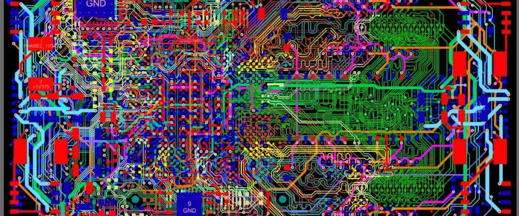
PCIE PCB Design Basics
PCIE Interface Overview
Peripheral Component Interconnect Express (PCIe) is a high-speed serial computer expansion bus standard. It is designed to replace the older PCI, PCI-X, and AGP bus standards. PCIe is used in a wide range of applications, including graphics cards, storage devices, network cards, and more.
PCIe uses a point-to-point topology, which means that each device has its own dedicated connection to the host. This allows for higher bandwidth and lower latency compared to shared buses. PCIe also supports multiple lanes, with each lane providing a specific amount of bandwidth.
PCIE PCB Design Guidelines
When designing a PCB for a PCIe device, there are several guidelines to follow to ensure proper functionality and signal integrity. Here are some of the key considerations:
-
Impedance Control: PCIe signals are high-speed and require controlled impedance traces to maintain signal integrity. Target impedance for PCIe traces is typically 85 ohms.
-
Signal Integrity: Proper signal integrity is critical for PCIe performance. Factors such as crosstalk, reflections, and noise can degrade signal quality and cause errors. Designers should follow best practices for high-speed design, such as minimizing trace length, using proper termination, and avoiding vias in critical signal paths.
-
Power Delivery: PCIe devices require both 3.3V and 12V power supplies. Designers should ensure that the power supplies are properly decoupled and that there is sufficient power delivery capacity.
-
Connector Placement: PCIe connectors should be placed close to the edge of the PCB to minimize trace length and reduce signal loss. It is also important to ensure that the connector pins are properly grounded.
-
Clocking: PCIe uses a differential clocking scheme to ensure proper synchronization between devices. Designers should ensure that clock traces are properly routed and that there is minimal skew between the clock and data signals.
In summary, designing a PCB for a PCIe device requires careful attention to signal integrity, power delivery, and connector placement. By following best practices for high-speed design and adhering to the PCIe specification, designers can ensure reliable and high-performance operation of their devices.
PCIE PCB Design Considerations

When designing a PCB for a PCI Express (PCIe) interface, there are several important considerations to keep in mind. These include power and grounding, signal integrity, PCB stackup, PCB layout, and PCB routing.
Power and Grounding
Proper power and grounding are essential for the reliable operation of a PCIe interface. It is important to ensure that the power supply is stable and that the ground plane is continuous. This can be achieved by using multiple vias to connect the ground plane to the power supply and ensuring that the power supply traces are wide enough to handle the current.
Signal Integrity
Signal integrity is critical for PCIe interfaces, as any noise or interference can cause data errors or even complete failure. To ensure signal integrity, it is important to minimize the length of the high-speed traces, use controlled impedance routing, and avoid sharp bends in the traces. Additionally, it is important to properly terminate the signals to prevent reflections.
PCB Stackup
The PCB stackup can have a significant impact on the performance of a PCIe interface. It is important to use a stackup that provides good isolation between the signal and power planes, as well as between different signal layers. It is also important to ensure that the impedance of the signal traces matches the impedance of the transmission line.
PCB Layout
The layout of the PCB can have a significant impact on the signal integrity and overall performance of a PCIe interface. It is important to group related signals together and minimize the length of the high-speed traces. Additionally, it is important to avoid crossing high-speed traces at right angles, as this can cause crosstalk and interference.
PCB Routing
Proper routing of the PCB is essential for the reliable operation of a PCIe interface. It is important to use controlled impedance routing and to ensure that the signal traces are properly terminated. Additionally, it is important to avoid routing high-speed traces near noisy components or near the edge of the PCB, where they can be more susceptible to interference.
Overall, designing a PCB for a PCIe interface requires careful attention to power and grounding, signal integrity, PCB stackup, PCB layout, and PCB routing. By following these guidelines, designers can ensure the reliable operation of their PCIe interfaces.
PCIE PCB Design Tools

PCB Design Software
PCB design software is essential for designing a PCIE PCB. These software tools provide a variety of features and functions that help designers create a high-quality design. Some popular PCB design software tools include Altium Designer, Eagle PCB, and KiCAD. These software tools are user-friendly and provide features such as schematic capture, PCB layout, and autorouting.
Simulation Tools
Simulation tools are also important for designing a PCIE PCB. These tools are used to simulate the behavior of the PCB and ensure that it meets the required specifications. Some popular simulation tools include LTSpice, PSpice, and Simulink. These tools allow designers to simulate the behavior of the PCB under different conditions and make changes to the design as needed.
In conclusion, PCB design software and simulation tools are essential for designing a high-quality PCIE PCB. These tools provide designers with the necessary features and functions to create a design that meets the required specifications.
PCIE PCB Design Best Practices
Design for Manufacturability
Designing a PCIE PCB with manufacturability in mind is crucial to ensure that the final product can be produced efficiently and with minimal errors. Some best practices to follow include:
- Keep it simple: Avoid using complex designs or components that may be difficult to manufacture. Instead, opt for simpler designs and components that are readily available and easy to assemble.
- Use standard materials: Using standard materials, such as FR-4, can help reduce costs and make it easier to find a manufacturer that can produce your PCB.
- Design for panelization: Panelizing your PCB can help reduce manufacturing costs by allowing multiple PCBs to be produced at once on a single panel.
- Minimize the number of layers: Using fewer layers can help reduce costs and make it easier to manufacture your PCB.
Design for Testability
Designing a PCIE PCB with testability in mind is important to ensure that the final product can be tested and verified for functionality. Some best practices to follow include:
- Design for test points: Adding test points to your PCB can make it easier to test and debug your design during the manufacturing process.
- Use built-in self-test (BIST) circuitry: Incorporating BIST circuitry into your design can help automate the testing process and reduce the need for manual testing.
- Ensure proper signal integrity: Proper signal integrity is crucial for ensuring that your design functions as intended. Using simulation tools, such as SPICE, can help ensure that your design meets signal integrity requirements.
By following these best practices for PCIE PCB design, you can help ensure that your final product is manufactured efficiently, tested thoroughly, and functions as intended.
