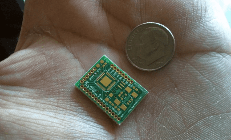
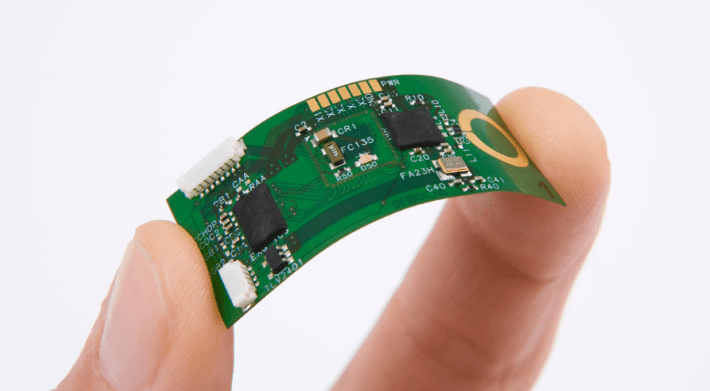
As technology keeps advancing, gadgets are becoming smaller. Also, as these gadgets become smaller, they will need some mini circuit boards before they function.
Furthermore, there’s nothing like the standard PCBs (printed circuit boards). Every board is made to suit an item. What this means is that the design of this circuit board is made to deliver a specific function in a particular space.
Our engineers at Hillman Curtis have been offering mini PCBs for different needs and industries for over 10 years. They offer competitive pricing as well as many offshore and domestic manufacturing options. Also, we deal in services which design for manufacturability, most especially when it comes to mini pcbs (mini printed circuit boards).
Some of the processes of our mini pcb manufacturing include apply solder paste, green solder mask, mounting holes, board design, etc.
In addition, circuit boards have very defined requirements. Fortunately, our professional manufacturing and engineering team has the ability to turn all concepts into reality. They can also test existing prototypes to ensure that all the needs of tolerance are met. When something goes out of specification, we at Hillman Curtis has what it takes to offer engineered solutions. With this, we can find solutions to your concerns, ensuring that you stay on budget and work with time.
It’s a great feeling when your electronic products get to the market very quickly. The mini circuit board service we offer are well designed to assist you in achieving that.
Circuit Boards Size Suitable for Mini Applications
The board size deals with the design. Also, you can utilize a specific design software, which could be computer-aided in creating your circuit layout. By doing so, you will be able to reduce the board’s size easily. Also, the spaces present between the two conducting paths are usually about 0.006 inches; it may be less too.
The dimensions of a printed circuit board have to do with the circuitry, as well as the enclosure, which houses the PCB. Also, it determines the fixed components as well as heat sinks of the circuit. Furthermore, utilizing the software, you will be able to reduce your board’s size easily. You should talk to your circuit manufacturer to assist you know the smaller possible mini PCB they will be able to manufacture.
In addition, the size of your circuit board size deals with the space available in the enclosure. In addition, if you will be designing tiny gadgets, then it is important to make use of mini circuit boards. However, take note that during the creation of your mini pcb design, there will be mini components in them as well. This could indicate soldering them using the soldering iron featuring fine tips, in addition to close-up glasses or microscope, especially whenever there are tight clearances in the holes.
Useful Tips in Making Mini PCBs
When you are designing the circuit, you have to look into some factors like text size, minimum silkscreen with, and minimum trace width, SMT minimum width the solder mask, minimum clearance solder mask, the minimum vias space/pads/trace, as well as the finish hole and drilling. All these factors are useful for knowing the least possible size of the circuit board.
In addition, always take note of the buried as well as blind vias carefully. This is so, because they have the ability to create a huge impact on the design coupled with engineering the PCB to be very mini. Vias help in connecting traces in-between the board layers. Also, the traditional options will end up decreasing the available routing space present on any circuit board.
More Tips

To ensure a routing space stays maximized as well as avoid the greater board size, and then we advise you to consider the alternatives. Also, blind vias assists in the connection of the external as well as internal layers having minimal spacing. Also, buried vias has the ability to connect the multiple layers found internally; however, they don’t reach out into its external layer. Now, this limits the total space requirement. It will also grant you a very stable product.
Also, you should consider the components spacing. If you decide to bring them extremely near to themselves, it may prevent the routing of traces. The more its pins present in that component, then the more its space that it will need or require. With proper spacing, it also ensures that the soldering of the components in the printed circuit board comes easy.
So also, there is a need for the components to stick to one general standard design for pin numbering. This is just to ensure the equal orientation of all. This then reduces the probability of any errors happening during soldering as well as inspections. Also, this could limit the manufacturing issues coupled with ensuring that everything is kept in mind during the size reduction.
In addition, expert engineers have the ability to assist you with determining the right width of the lines, with respect to the current utilized during the application. Larger lines might take more space; however, this will reduce the PCB’s heat relative to the dissipation.
Also, size lines with respect to current will ensure your mini PCBs run smoothly without requiring extra cooling support.
What are the Benefits of the Mini PCB
Room saving
As we have explained earlier, one great benefit is that these mini circuits are usually space-efficient. What this means is that they aren’t gigantic and bulky. Smartphones as well as other small device or devices have these circuits present in them.
Furthermore, assembling these printed circuit boards comes easy. This is due to its higher feasibility degree provided by these circuits. In addition, these mini circuits provide extra space to allow the proper fitting of the other components into the electronics.
Lower cost
The miniaturization process makes use of the mini circuits. As a result of this, these devices will become very cost-efficient for the clients. Also, the materials for production are also affordable. This also holds for transportation as things become easier for both producers and suppliers.
Furthermore, smaller production equipment requires affordable and easy transportation. In addition, the production of circuit boards doesn’t come at a high price with respect to the budget. This way, the mini circuits will provide many benefits to help in reducing the costs.
Environmentally-friendly products
The products are environmentally friendly. Materials required for the whole production aren’t many. Therefore, these few materials or components won’t cause any negative effects on environments. Furthermore, when the materials are fewer, the less wastes will be. Some manufacturers involved in bulk manufacturing have been negligent when it comes to waste generated. This has caused some threats for the PCB industry.
Efficiency
With respect to mini circuit boards, they are clearly unmatched. Furthermore, heat dissipation via the circuit boards is less impressive. This could be another significant reason for their great use in electronics. As a result of low dissipation, they provide electrical and thermal characteristics to all the devices that they are utilized for.
How to Reduce the Mini PCB Size
Three main ways are helpful for reducing your PCB and then transforming it to take the desired shape of mini PCB with little effort.
Removing the testing tools
Removing the testing tools could help in reducing the size of circuit boards. The initial components of the circuits as well as the other tools required for error removal and debugging purposes takes much space. This is why these circuits’ size will not reduce. With respect to reduction in size, the tools for testing, such as these require secure removal. As of today, a good number of circuits don’t require some of these parts.
Usage of the Multilayer Circuit Boards
There are prototypes having at least one layer in their layouts during the circuit designs. All these offer some benefits when having a very easy reach to these traces and counterparts that are available in the circuitry. These advantages include repair, remodification, and inspection.
Once the mini PCB layout has been approved, then it requires a size reduction immediately. Note that, the adjusting of these components must be done carefully to prevent any possible setbacks. This is the major reason why the use of multilayer circuits is necessary. This is because they only take little space and they handle their tasks smoothly.
Wi-Fi Bluetooth Combo Module
The Wi-Fi Bluetooth combo module comes with its benefits as well as pitfalls when it comes to PCB size reduction. This involves the modifications that relate to power conversions or transformations, wireless connections, and circuit boards.
The step is important for designing printed circuits. This could be expensive and affordable, which is dependent on the circuit board type. This process also functions with the Wi-Fi and Bluetooth interlinking with one model using an antenna.
Conclusion
Hillman Curtis is an experienced manufacturer of mini PCBs (mini printed circuit board). We focus much on perfect customer services and industry tolerances. Also, we provide a complete one-stop shop, which can adjust quickly to meet both low and high volume demands that you may have for the mini printed circuit boards.
Contact us today so that we can learn more regarding the way we can help you design the best mini pcb at low cost that suits your needs and requirements.
