PCB design is an essential component of modern electronics. A printed circuit board (PCB) is a board that connects electronic components through conductive tracks, pads, and other features etched from copper sheets laminated onto a non-conductive substrate. The design of a PCB is critical to the functionality of electronic devices, as it determines how components are connected and how signals are transmitted.
The process of designing a PCB begins with a schematic diagram, which outlines the electrical connections between components. The schematic is then translated into a physical layout, which determines the size, shape, and placement of components on the board. PCB design software is used to create the layout, which can be refined through iterative testing and simulation. Once the design is finalized, it is sent to a manufacturer to be produced. PCB design is a complex and specialized field that requires knowledge of electronics, physics, and engineering. A well-designed PCB can improve the performance and reliability of electronic devices, making it a crucial aspect of modern technology.
Basics of PCB Design from Schematic
PCB design from schematic is a crucial step in the process of creating a functional electronic device. It involves translating a schematic diagram into a physical printed circuit board that can be manufactured and assembled into a final product. Here are some basics of PCB design from schematic:
1. Component Placement
The first step in PCB design from schematic is component placement. This involves deciding where to place each component on the board. It is important to consider factors such as signal flow, power distribution, and thermal management when placing components. Components should be placed in a way that minimizes noise and interference and ensures proper functionality of the circuit.
2. Traces and Routing
Once the components are placed, the next step is to route the traces between them. Traces are the conductive pathways that connect the various components on the PCB. Traces should be routed in a way that minimizes signal loss, noise, and interference. It is important to consider factors such as trace width, spacing, and length when routing traces.
3. Grounding and Power Planes
Grounding and power planes are an important part of PCB design from schematic. Ground planes provide a low-impedance path for return currents and help reduce noise and interference. Power planes provide a stable voltage supply to the components on the PCB. It is important to ensure that the grounding and power planes are properly connected and that there are no breaks or gaps in the planes.
4. Design for Manufacturability
Finally, it is important to design the PCB for manufacturability. This involves ensuring that the PCB can be manufactured and assembled efficiently and cost-effectively. It is important to consider factors such as panelization, solder mask, and silkscreen when designing the PCB.
In conclusion, PCB design from schematic is a complex process that requires careful consideration of many factors. By following these basics of PCB design from schematic, you can create a functional and reliable PCB that meets the requirements of your electronic device.
Creating a Schematic
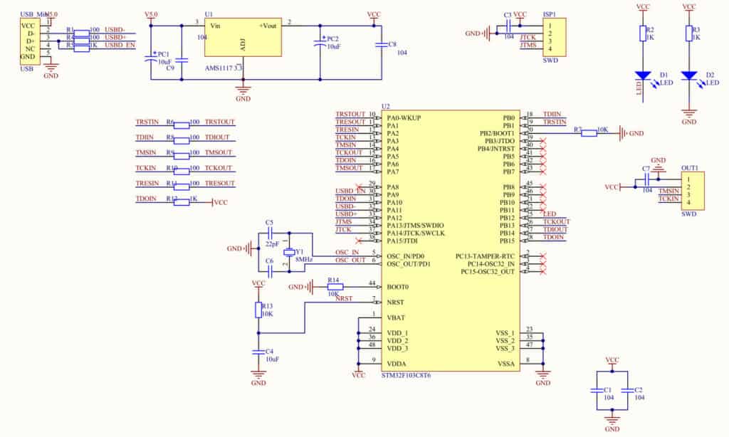
When designing a printed circuit board (PCB), the first step is to create a schematic. The schematic is a graphical representation of the circuit, showing all the components and their connections. It is a blueprint for the PCB layout, and it is essential to get it right before moving on to the layout stage.
To create a schematic, you will need a schematic capture tool. There are many options available, both free and paid, such as Eagle, Altium, KiCad, and more. Choose one that suits your needs and level of expertise.
Once you have your schematic capture tool, start by placing the components on the schematic. You can do this manually or use a library of pre-made components. Make sure to choose components that are suitable for your circuit and meet your requirements.
Next, connect the components using wires or buses. You can also use net labels to connect components that are not physically close to each other. It is essential to keep the schematic neat and organized, as it will make it easier to read and understand.
Finally, add any necessary annotations, such as values, part numbers, and reference designators. This information will be used later in the layout stage to place the components on the PCB.
In summary, creating a schematic is the first step in designing a PCB. It involves placing components, connecting them, and adding annotations. It is essential to get it right before moving on to the layout stage, as any mistakes in the schematic will be carried over to the PCB layout.
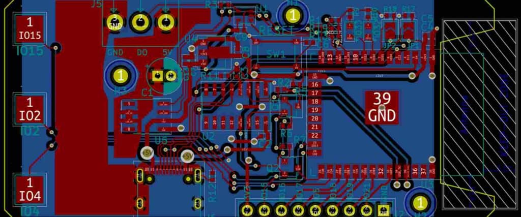
PCB Layout Design
PCB layout design is a crucial part of the PCB design process. It involves the placement and routing of electronic components on the PCB to ensure that the circuit functions as intended. The PCB layout design is critical to the performance, reliability, and manufacturability of the final product.
In the PCB layout design, the designer must consider various factors, such as the size and shape of the PCB, the number and type of components, and the electrical characteristics of the circuit. The designer must also consider the manufacturing process and ensure that the design is manufacturable and cost-effective.
To ensure that the PCB layout design is accurate, designers use specialized software tools that allow them to create a virtual representation of the PCB. These tools enable the designer to place and route components, define the electrical connections between them, and check for errors and design rule violations.
During the PCB layout design process, designers must also consider the thermal and mechanical aspects of the design. They must ensure that the PCB can dissipate heat effectively and that it can withstand the stresses of the environment in which it will be used.
In conclusion, the PCB layout design is a critical step in the PCB design process. It requires careful consideration of various factors, including the size and shape of the PCB, the number and type of components, the electrical characteristics of the circuit, and the manufacturing process. With the use of specialized software tools, designers can create an accurate and manufacturable design that meets the requirements of the circuit.
Design Rule Check (DRC)

Design Rule Check (DRC) is an essential step in the PCB design process. It is a software tool that checks the design against a set of pre-defined rules to ensure that the design meets the manufacturing requirements. The DRC tool checks for errors such as short circuits, open circuits, and spacing violations.
The DRC tool can be configured to check for specific design rules, such as minimum trace width, minimum clearance, and minimum annular ring size. The tool can also check for specific design requirements, such as impedance matching and differential pair routing.
DRC is an important step in the design process because it helps to identify errors early in the design cycle. This helps to reduce the number of design iterations required, which in turn reduces the time and cost of the design process.
In conclusion, DRC is an essential tool in the PCB design process. It helps to ensure that the design meets the manufacturing requirements and reduces the number of design iterations required.
Gerber File Generation
Once the PCB design is complete and the schematic is converted into a PCB layout, the next step is to generate Gerber files. Gerber files are the standard file format used to communicate the PCB design to the PCB manufacturer.
Gerber files contain all the necessary information about the PCB design, such as the copper traces, component placement, drill holes, and board outline. PCB manufacturers use these files to create the physical PCB board.
To generate Gerber files, most PCB design software has an in-built Gerber file generator. The software will generate a set of files, each representing a different layer of the PCB design. These layers include the top copper layer, bottom copper layer, solder mask layer, silkscreen layer, and drill files.
It is important to ensure that the Gerber files generated are accurate and complete. Any errors or missing information can lead to manufacturing defects or incorrect PCBs. It is recommended to double-check the generated Gerber files before sending them to the manufacturer.
In addition to the Gerber files, some PCB manufacturers may also require other files such as a bill of materials (BOM) and assembly drawings. These files provide additional information about the components used in the PCB design and their placement on the board.
In conclusion, generating accurate and complete Gerber files is crucial for successful PCB manufacturing. PCB design software makes this process simple and straightforward, but it is important to double-check the files before sending them to the manufacturer.
