PCB design is a crucial aspect of electronic engineering, and software tools like KiCad have made it easier and more accessible than ever before. KiCad is an open-source software suite that provides a comprehensive set of tools for designing printed circuit boards (PCBs). With its intuitive interface and powerful features, KiCad has become a popular choice for hobbyists and professionals alike.
One of the key advantages of KiCad is its flexibility. The software allows users to design PCBs with a wide range of components, from simple circuits to complex systems. KiCad provides a library of pre-built components, and users can also create their own custom components. This flexibility makes KiCad a powerful tool for a variety of applications, from prototyping to production.
Basics of PCB Design in KiCad
KiCad is a popular open-source software tool for designing printed circuit boards (PCBs). PCB design is the process of creating a layout for a circuit board that will be used to manufacture the final product. Here are some basics of PCB design in KiCad:
Schematic Capture
The first step in designing a PCB in KiCad is to create a schematic. This schematic captures the electrical connections between components in the circuit. KiCad provides a user-friendly interface that allows you to add components, connect them together, and annotate the schematic.
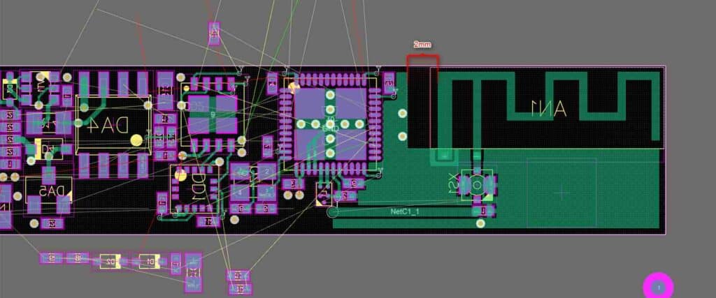
PCB Layout
Once the schematic is complete, the next step is to create the PCB layout. This involves placing the components on the board and routing the electrical connections between them. KiCad provides a powerful set of tools for creating the PCB layout, including automatic and manual routing modes.
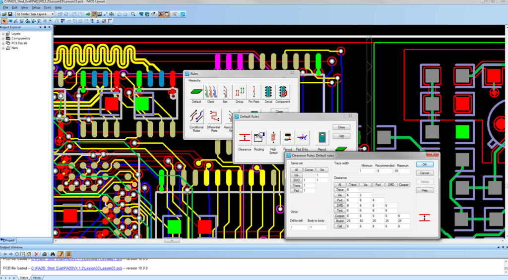
Design Rules
Design rules are a set of constraints that define the minimum spacing and clearance requirements for components and traces on the PCB. KiCad provides a comprehensive set of design rules that can be customized to meet your specific needs.
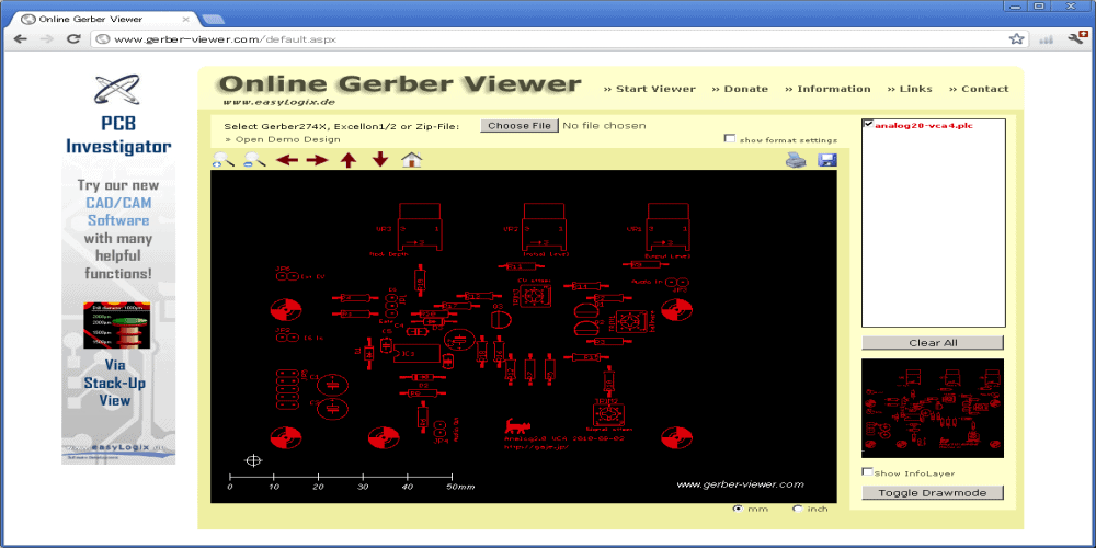
Gerber Files
Gerber files are the industry-standard format for PCB manufacturing. KiCad allows you to generate Gerber files for your PCB design, which can be sent to a manufacturer for production.
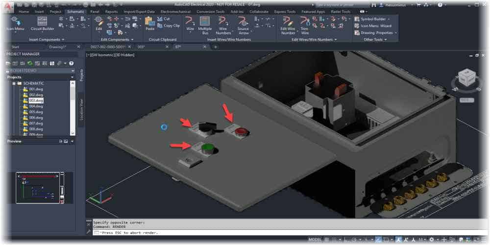
3D Visualization
KiCad provides a 3D visualization tool that allows you to visualize your PCB design in three dimensions. This can be useful for identifying potential issues with component placement and clearance.
Overall, KiCad is a powerful and flexible tool for designing PCBs. With its user-friendly interface, comprehensive set of design rules, and powerful visualization tools, KiCad is an excellent choice for both beginners and experienced PCB designers.
KiCad Schematic Editor

The KiCad Schematic Editor is a powerful tool for designing and documenting electronic circuits. It allows you to create and edit schematics, add components and symbols, and connect them together using wires and buses.
One of the key features of the KiCad Schematic Editor is its ability to handle complex projects with ease. You can create hierarchical designs, where sub-circuits are represented by blocks that can be reused in other parts of the circuit. This makes it easy to manage large projects and keep track of all the connections.
Another great feature is the ability to create custom symbols and footprints. You can create your own symbols for components that are not included in the default libraries, or modify existing symbols to suit your needs. The same goes for footprints, which are used to represent the physical layout of components on a PCB.
The KiCad Schematic Editor also has a comprehensive set of tools for checking your design for errors and inconsistencies. You can run a Design Rule Check (DRC) to ensure that all your connections are correct and that there are no overlapping components or nets. You can also run a Netlist Check to ensure that your schematic is compatible with your PCB layout.
Overall, the KiCad Schematic Editor is a powerful and flexible tool for designing electronic circuits. Whether you are a beginner or an experienced designer, it has everything you need to create professional-quality schematics for your projects.
KiCad PCB Layout Editor
KiCad is a popular open-source software suite for electronic design automation (EDA). It offers a range of tools for designing printed circuit boards (PCBs), including a schematic editor and a PCB layout editor. In this section, we’ll focus on the PCB layout editor.
The KiCad PCB layout editor is a powerful tool that allows you to create and edit PCB designs with ease. It offers a range of features and functions that make it an ideal choice for both beginners and experienced designers.
Some of the key features of the KiCad PCB layout editor include:
-
Intuitive user interface: The KiCad PCB layout editor has a user-friendly interface that is easy to navigate. You can access all the tools and functions you need from the toolbar or menu bar.
-
Design rule checking: The KiCad PCB layout editor includes a design rule checking (DRC) tool that helps you ensure your design meets the required specifications and standards.
-
Footprint editor: The KiCad PCB layout editor includes a built-in footprint editor that allows you to create custom footprints for your components.
-
3D visualization: The KiCad PCB layout editor offers a 3D visualization tool that allows you to view your design in three dimensions, which can help you identify any potential issues before you send your design to production.
Overall, the KiCad PCB layout editor is a powerful and versatile tool that can help you create high-quality PCB designs quickly and easily. Whether you’re a beginner or an experienced designer, the KiCad PCB layout editor has everything you need to bring your electronic designs to life.
Creating Footprints in KiCad
Creating custom footprints is a crucial part of PCB design, as it allows you to add components that are not already included in KiCad’s library. In this section, we will go over the steps to create a custom footprint in KiCad.
-
Open the Footprint Editor: To create a new footprint, open the Footprint Editor by clicking on the “Create a new footprint” button in the main KiCad window.
-
Select the Component: After opening the Footprint Editor, select the component for which you want to create a footprint. You can either choose from the existing components in KiCad’s library or create a new component.
-
Create the Footprint: Once you have selected the component, start creating the footprint by using the various tools available in the Footprint Editor. You can use the “Add Pad” tool to add pads to the footprint, and the “Add Graphic Line” tool to add graphic lines.
-
Save the Footprint: After creating the footprint, save it by clicking on the “Save” button in the Footprint Editor. You can also save the footprint as a new component in KiCad’s library by selecting “Save as new component” in the “File” menu.
-
Use the Footprint: Once you have created the footprint, you can use it in your PCB design by adding the component to your schematic and assigning the footprint to the component.
In conclusion, creating custom footprints in KiCad is a straightforward process that can greatly enhance your PCB design capabilities. By following the steps outlined above, you can create custom footprints for any component that is not already included in KiCad’s library.
Design Rule Checking in KiCad
Design Rule Checking (DRC) is an essential step in the PCB design process, ensuring that the design meets the manufacturing requirements and is free from errors. KiCad has a built-in DRC tool that can check the design against a set of rules defined by the user.
To access the DRC tool in KiCad, go to the “Tools” menu and select “DRC”. The DRC dialog box will appear, where you can specify the rules to check and the parameters for each rule.
KiCad’s DRC tool checks for various design rule violations, such as minimum clearance, minimum track width, and overlapping pads. The tool also checks for errors related to the drill holes, solder mask, and silkscreen layers.
The DRC results are displayed in the “Messages” panel, where you can see a list of errors and warnings. You can double-click on an error to highlight the offending object in the design view.
To customize the DRC rules in KiCad, go to the “PCB Rules and Constraints Editor” in the “Tools” menu. Here, you can define the rules for each layer, such as the minimum clearance, minimum track width, and drill hole size.
In conclusion, KiCad’s DRC tool is a powerful feature that helps ensure the design meets the manufacturing requirements and is free from errors. By customizing the DRC rules, you can tailor the tool to your specific design needs and catch potential errors before they become costly mistakes.
Generating Gerber Files in KiCad
After designing your PCB in KiCad, the next step is to generate Gerber files. Gerber files are a standard format that PCB manufacturers use to create the physical PCB. Here’s how to generate Gerber files in KiCad:
- Click on the “Plot” icon in the toolbar or go to File > Plot.
- In the Plot window, select the layers you want to plot. By default, all layers are selected, but you can uncheck the ones you don’t need.
- Choose the output directory where you want to save the Gerber files.
- Click on the “Plot” button to generate the Gerber files.
It’s important to note that you should always double-check the generated Gerber files before sending them to the manufacturer. You can use a Gerber viewer to make sure everything looks correct.
In addition to the Gerber files, you should also generate a drill file. The drill file contains information about the holes that need to be drilled in the PCB. To generate a drill file in KiCad:
- Click on the “Drill” icon in the toolbar or go to File > Fabrication Outputs > Excellon Drill File.
- Choose the output directory where you want to save the drill file.
- Click on the “Generate Drill File” button.
Once you have the Gerber files and drill file, you can send them to the manufacturer to create your PCB. By following these steps, you can ensure that your PCB design is correctly translated into physical form.
Advanced Techniques in KiCad
KiCad is a powerful PCB design tool that offers a range of advanced techniques to help you create complex and professional designs. Here are some of the advanced techniques you can use in KiCad:
-
Hierarchical design: This technique allows you to create complex designs by breaking them down into smaller, more manageable sub-designs. You can then link these sub-designs together to create a complete system. This technique is particularly useful for large designs with many components.
-
Custom footprints: KiCad comes with a large library of pre-defined footprints, but you can also create your own custom footprints. This is useful if you are using a component that is not in the library or if you want to create a custom shape for a component.
-
3D visualization: KiCad allows you to create 3D models of your PCB designs, which can be useful for visualizing how the components fit together and for checking for any potential clearance issues.
-
Design rule checking: KiCad has a powerful design rule checking system that can help you ensure that your design meets your specific requirements. You can set up rules for things like minimum trace width, minimum clearance between components, and more.
-
Interactive routing: KiCad’s interactive routing feature allows you to create complex routing patterns quickly and easily. You can also set up routing rules to ensure that your design meets your specific requirements.
Overall, KiCad offers a range of advanced techniques that can help you create complex and professional PCB designs. By taking advantage of these techniques, you can create designs that are both functional and aesthetically pleasing.
Conclusion
In conclusion, KiCad is a powerful and flexible tool for PCB design. With its open-source nature, it is accessible to anyone who wants to learn and use it. Here are some key takeaways from this article:
- KiCad offers a comprehensive set of tools for schematic capture, PCB layout, and design rule checking.
- The software is free to use, and its open-source nature means that users can contribute to its development and improvement.
- KiCad supports a wide range of file formats, making it easy to collaborate with others and import/export designs to other software.
- The software is constantly evolving, with new features and improvements being added regularly.
- While KiCad has a bit of a learning curve, there are many resources available online to help users get started and become proficient with the software.
Overall, KiCad is a great choice for anyone looking to design PCBs, whether you’re a hobbyist or a professional. With its powerful features, open-source nature, and active community, it’s a tool that can help you bring your ideas to life.
