PCB design solutions are essential for creating high-quality printed circuit boards that meet specific requirements. PCB design solutions can include software, hardware, and services that help designers create and test their designs. These solutions can help designers streamline their workflow, reduce errors, and improve the overall quality of their designs.
One of the main advantages of using PCB design solutions is that they can help designers create more complex designs in less time. These solutions can automate many of the design processes, such as routing, placement, and verification, which can save designers a significant amount of time. Additionally, these solutions can help designers identify and fix errors before the board is manufactured, which can save time and money in the long run.
Another advantage of using PCB design solutions is that they can provide designers with access to advanced design features and technologies. For example, some solutions may include advanced routing algorithms that can help designers optimize their designs for signal integrity or reduce crosstalk. Other solutions may include simulation tools that can help designers test their designs under different conditions and identify potential issues before the board is manufactured.
PCB Design Solutions
PCB design solutions are critical for creating high-quality printed circuit boards that meet the needs of modern electronics. These solutions include a variety of tools and techniques that help designers create PCBs that are reliable, efficient, and cost-effective.
Design Software
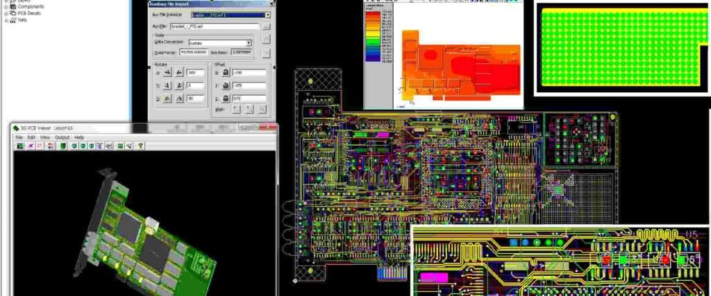
Design software is an essential tool for PCB designers. With the right software, designers can create and test their designs quickly and accurately. Some popular PCB design software options include Altium Designer, Eagle PCB, and KiCAD.
Component Selection
Selecting the right components for a PCB is crucial for ensuring that the board functions correctly and meets the needs of the end-user. Designers need to consider factors such as component quality, availability, and cost when selecting components.
Layout and Routing
The layout and routing of a PCB can have a significant impact on its performance and reliability. Designers need to consider factors such as signal integrity, power distribution, and thermal management when laying out and routing a PCB.
Manufacturing and Assembly
Manufacturing and assembly are critical stages in the PCB design process. Designers need to consider factors such as manufacturing capabilities, assembly processes, and testing procedures when designing a PCB for manufacturing.
In conclusion, PCB design solutions are essential for creating high-quality printed circuit boards that meet the needs of modern electronics. Design software, component selection, layout and routing, and manufacturing and assembly are all critical components of a successful PCB design process.
Design Software
Overview of Popular Software
When it comes to PCB design software, there are several popular options available in the market. Some of the most widely used software include Altium Designer, Eagle PCB, KiCAD, and OrCAD. Each software has its own set of features and capabilities, making it suitable for different types of PCB designs.
Altium Designer is a comprehensive software that allows users to design complex PCBs with ease. It offers a range of advanced features such as schematic capture, PCB layout, and 3D visualization. Eagle PCB is another popular software that is known for its user-friendly interface and extensive library of components. KiCAD is an open-source software that is free to use and offers a range of tools for schematic capture, PCB layout, and 3D visualization. OrCAD is a powerful software that offers advanced features such as signal integrity analysis, power analysis, and thermal analysis.
Comparison of Features and Capabilities
When choosing a PCB design software, it is important to compare the features and capabilities of each software to determine which one is best suited for your needs. Altium Designer offers a comprehensive set of features that allow users to design complex PCBs with ease. It offers advanced features such as schematic capture, PCB layout, and 3D visualization. Eagle PCB is known for its user-friendly interface and extensive library of components. KiCAD is a free and open-source software that offers a range of tools for schematic capture, PCB layout, and 3D visualization. OrCAD is a powerful software that offers advanced features such as signal integrity analysis, power analysis, and thermal analysis.
Cost and Licensing Options
The cost and licensing options of PCB design software vary depending on the software and the vendor. Altium Designer is a commercial software that offers a range of licensing options, including perpetual and subscription licenses. Eagle PCB offers a range of licensing options, including free, standard, and professional licenses. KiCAD is a free and open-source software that can be downloaded and used for free. OrCAD is a commercial software that offers a range of licensing options, including perpetual and subscription licenses.
Overall, when choosing a PCB design software, it is important to consider the features, capabilities, and cost of each software to determine which one is best suited for your needs.
Component Selection

Understanding Component Requirements
When designing a PCB, it is essential to select the right components that meet the specific requirements of the project. The first step in the component selection process is to understand the requirements of the circuit. This includes determining the voltage, current, and power requirements of the circuit, as well as the environmental conditions the circuit will be subjected to.
Sourcing Components and Suppliers
Once you have determined the requirements of the circuit, the next step is to source the components and suppliers. It is essential to work with reputable suppliers who can provide high-quality components that meet the requirements of the circuit. When sourcing components, it is also important to consider the availability of the components, lead times, and cost.
Verification and Testing
After selecting and sourcing the components, it is crucial to verify and test them to ensure they meet the requirements of the circuit. This includes checking the specifications of the components against the requirements of the circuit and testing the components for functionality and reliability. It is also important to verify that the components are compatible with the other components in the circuit.
In summary, selecting the right components is a critical part of the PCB design process. By understanding the requirements of the circuit, sourcing components and suppliers, and verifying and testing the components, you can ensure that your PCB design solution meets the specific needs of your project.
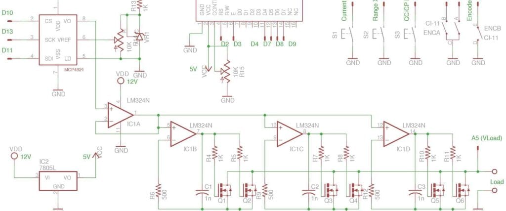
Layout and Routing
Design Considerations and Best Practices
When designing a PCB layout, it is important to consider factors such as signal integrity, power distribution, and thermal management. A well-designed layout can help reduce noise and interference, improve signal quality, and ensure reliable operation of the circuit.
Some best practices to keep in mind include:
- Minimizing the length of signal traces to reduce signal degradation and noise.
- Placing decoupling capacitors close to power and ground pins to reduce noise and improve power distribution.
- Keeping high-speed signals away from noisy components and traces.
- Ensuring adequate spacing between traces to minimize crosstalk.
- Using copper pour to improve thermal management and reduce EMI/EMC.
Tools and Techniques for Efficient Routing
Efficient routing can save time and reduce errors in the PCB design process. Some tools and techniques that can be used include:
- Auto-routing software to automatically generate a layout based on predefined rules and constraints.
- Interactive routing to manually route specific traces while taking into account design constraints.
- Differential pair routing to ensure consistent signal quality and minimize crosstalk.
- Net highlighting to visually identify and trace specific nets throughout the design.
Signal Integrity and EMI/EMC Compliance
Signal integrity and EMI/EMC compliance are critical factors in PCB design. Poor signal integrity can lead to signal degradation, while EMI/EMC issues can cause interference with other devices and affect overall system performance.
To ensure signal integrity and EMI/EMC compliance, it is important to:
- Use proper termination techniques for high-speed signals to minimize reflections and signal degradation.
- Implement shielding and filtering techniques to reduce EMI/EMC.
- Ensure proper grounding and power distribution throughout the design.
- Use simulation tools to analyze and optimize signal integrity and EMI/EMC performance.
Overall, careful consideration of layout and routing can help ensure a reliable and high-performing PCB design.
Manufacturing and Assembly
DFT and DFM Guidelines
Design for Testability (DFT) and Design for Manufacturing (DFM) guidelines are essential in ensuring that the PCB design can be easily manufactured and assembled with minimal errors. DFT guidelines help ensure that testing can be performed efficiently and effectively, while DFM guidelines ensure that the design can be manufactured with minimal waste and errors. Some common DFT guidelines include the use of test points, proper labeling of components, and avoiding the use of vias under components. DFM guidelines include the use of standard PCB sizes, proper spacing between components, and avoiding the use of complex shapes.
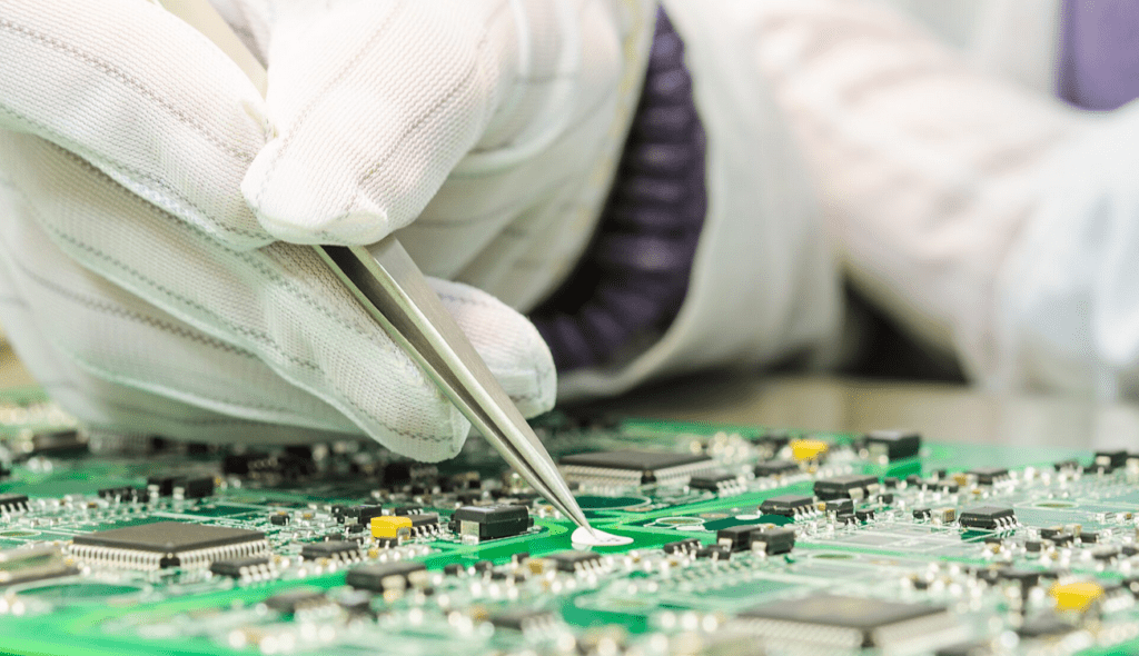
PCB Fabrication and Assembly Processes
PCB fabrication involves the process of creating the physical PCB from a design file. This process involves several steps, including drilling, plating, and etching. Once the PCB is fabricated, it can then be assembled with components. PCB assembly involves placing components on the board, soldering them in place, and performing any necessary testing. There are several methods for PCB assembly, including through-hole, surface mount, and mixed technology.
Quality Control and Testing
Quality control and testing are critical in ensuring that the final product meets the necessary specifications and requirements. Quality control involves inspecting the PCB and components for defects and ensuring that they meet the necessary standards. Testing involves verifying that the PCB functions correctly and meets the necessary performance requirements. Some common testing methods include functional testing, in-circuit testing, and boundary scan testing.
In summary, proper DFT and DFM guidelines, effective PCB fabrication and assembly processes, and thorough quality control and testing are all essential in ensuring that the PCB design can be easily manufactured and assembled with minimal errors.
