Printed circuit board (PCB) layout CAD software is a crucial tool for designing and manufacturing electronic devices. The software allows designers to create a virtual representation of the PCB, which can then be used to test and optimize the design before it is sent for production. PCB layout CAD software has become increasingly popular in recent years due to the rise of the Internet of Things (IoT) and the growing demand for smaller and more complex electronic devices.
One of the primary benefits of using PCB layout CAD software is that it allows designers to create highly complex PCBs with ease. The software provides a range of tools and features that make it easy to place components, trace connections, and optimize the layout for maximum performance. Additionally, the software can automatically generate manufacturing files, such as Gerber files, which can be used to create the physical PCB. This streamlines the design process and reduces the likelihood of errors or delays in production.
Overall, PCB layout CAD software is an essential tool for anyone involved in the design and manufacture of electronic devices. It allows designers to create highly complex PCBs with ease, while also streamlining the design process and reducing the likelihood of errors or delays in production. As the demand for smaller and more complex electronic devices continues to grow, the importance of PCB layout CAD software will only increase.
PCB Layout CAD Software
Overview
PCB layout CAD software is an essential tool for designing printed circuit boards. It allows designers to create schematics and board layouts, place components, route traces, and generate manufacturing files. PCB layout CAD software has become increasingly sophisticated over the years, with many powerful features and options available to users.
Popular PCB Layout CAD Software
There are many PCB layout CAD software options available, each with its own strengths and weaknesses. Some of the most popular options include:
Features
PCB layout CAD software typically includes a range of features to help designers create high-quality boards. Some of the most common features include:
- Schematic capture: Allows designers to create and edit schematics for their PCBs.
- Component placement: Enables designers to place components on the board and adjust their position as needed.
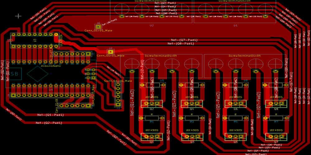
- Trace routing: Helps designers route traces between components to create connections on the board.
- Design rule checking: Verifies that the design meets certain rules and standards, such as minimum trace widths and clearances.
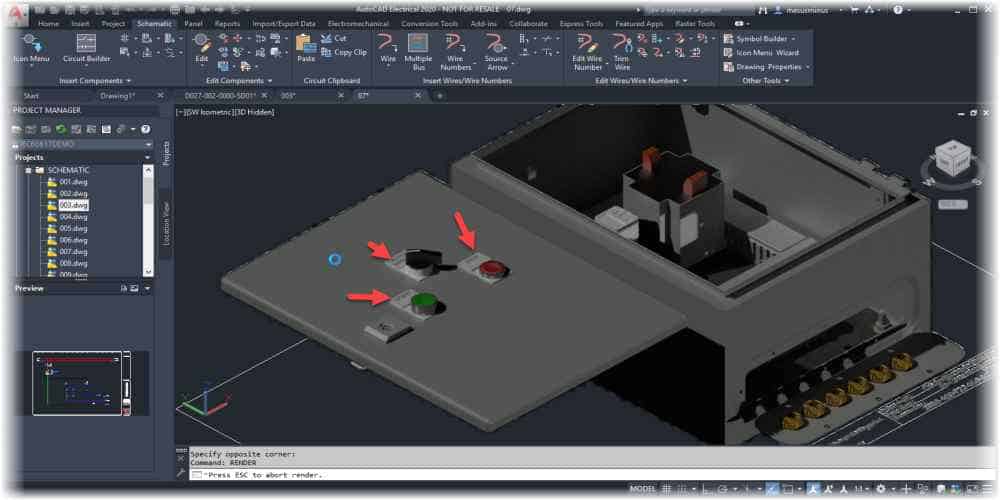
- 3D visualization: Allows designers to view their board in 3D and check for potential issues with component placement or clearance.
- Manufacturing file generation: Generates files needed for manufacturing the board, such as Gerber files and drill files.
Overall, PCB layout CAD software is an essential tool for anyone designing printed circuit boards. With many powerful features and options available, designers can create high-quality boards quickly and efficiently.
Designing PCB Layouts

PCB Layout Design Process
The PCB layout design process involves several steps that must be followed to ensure a successful design. The following are the key steps involved in the process:
-
Schematic capture: This step involves creating a schematic diagram of the circuit design using a schematic capture tool.
-
Component placement: In this step, the components are placed on the board according to their functions and their interconnections.
-
Routing: This step involves routing the connections between the components using a routing tool.
-
Design rule check: This step involves checking the design against the design rules to ensure that the design meets the required specifications.
-
Gerber generation: This step involves generating the Gerber files, which are used to manufacture the PCB.
Design Considerations
When designing a PCB layout, there are several design considerations that must be taken into account. These considerations include:
-
Signal integrity: This refers to the quality of the signal that is transmitted through the PCB. To ensure good signal integrity, the layout must be designed to minimize noise and interference.
-
Power distribution: The layout must be designed to distribute power to the components in an efficient and effective manner.
-
Thermal management: The layout must be designed to dissipate heat generated by the components effectively.
-
Mechanical constraints: The layout must be designed to fit within the mechanical constraints of the device.
Layout Techniques
There are several layout techniques that can be used to improve the performance of the PCB. These techniques include:
-
Ground plane: A ground plane can be used to reduce noise and interference by providing a low-impedance ground path.
-
Signal routing: Signal routing can be optimized to minimize crosstalk and noise.
-
Component placement: Component placement can be optimized to reduce the length of the traces and improve signal integrity.
-
Via placement: Via placement can be optimized to reduce the number of vias and improve signal integrity.
-
Copper pour: Copper pour can be used to improve thermal management and reduce noise and interference.
In conclusion, designing a PCB layout requires careful consideration of the design process, design considerations, and layout techniques. By following these steps and techniques, designers can create high-quality PCB layouts that meet the required specifications.
PCB Layout CAD Tools
Types of PCB Layout CAD Tools
PCB Layout CAD tools are software programs that are used to design and layout printed circuit boards (PCBs). There are various types of PCB Layout CAD tools available in the market, ranging from free open-source software to commercial software with advanced features. Some of the commonly used PCB Layout CAD tools are:
- Altium Designer
- Eagle PCB Design
- KiCad
- OrCAD PCB Designer
- PADS PCB Design
- CircuitMaker
- DipTrace
Each of these tools has its own strengths and weaknesses, and the choice of tool depends on factors such as the complexity of the design, budget, and personal preference.
Comparison of PCB Layout CAD Tools
When choosing a PCB Layout CAD tool, it is important to compare the features and capabilities of different tools to make an informed decision. Some of the factors to consider when comparing PCB Layout CAD tools are:
- User interface and ease of use
- Library of components
- Design rule checking (DRC)
- Signal integrity analysis
- 3D visualization
- Support for multi-layer PCBs
- Price
Best Practices for Using PCB Layout CAD Tools
To make the most of PCB Layout CAD tools, it is important to follow some best practices. Some of the best practices for using PCB Layout CAD tools are:
- Start with a clear understanding of the design requirements
- Use a consistent naming convention for components and nets
- Follow the design rules and guidelines
- Use the design rule checking (DRC) feature to catch errors early
- Test the design thoroughly before sending it for fabrication
By following these best practices, designers can ensure that their PCB Layout CAD tool is used effectively and efficiently, resulting in a high-quality PCB design.
Overall, the choice of PCB Layout CAD tool depends on the specific requirements of the project and the designer’s preference. By comparing different tools and following best practices, designers can create high-quality PCB designs that meet their requirements.
