KiCad is a PCB design software with advanced features for PCB design. This PCB design software is free and open. PCB designers consider KiCad as a very mature software that aids the successful development of complex electronic boards. Also, this software doesn’t have any limitation when it comes to board size. Therefore, it can handle about 32 copper layers, 4 auxiliary layers and about 14 technical layers.
This KiCad tutorial will use a KiCad project as an example. Here, we will go through schematic capture, PCB layout, and also, discuss editing and library linking. Although this KiCad tutorial mainly focuses on beginners, we will use terms like polygon pours and schematic symbols.
What is kiCad?
KiCad is a software specially created to handle anything that involves PCB designing. Also, this free and open software comes with advanced features that help PCB designers to achieve success. This sophisticated software is extensively integrated by both professionals and hobbyists. One of the benefits of KiCad is that it is available for use in several platforms like macOS, Windows, and Ubuntu.
KiCad developers have continually introduced new features and upgraded the existing ones over the years. This PCB design software has undergone 5 major versions. Also, it has evolved to be a great alternative to commercial products.
Design Tools of KiCad Suite
KiCad Suite has a lot design tools. These tools are responsible for the performance of this software.
Symbol Editor
A schematic is a graphical representation of components and their interconnections. Also, a symbol editor develops new schematic symbols that are not in the libraries. For instance, if you are developing a new symbol for an IC, you can specify the pinouts and properties. Also, you can then save this symbol to a new library or an existing one.
Image converter
The image converter is handy when you need to include custom logos that aren’t available in the libraries to your circuit board. KiCad supports only vector formats. Therefore, you can import raster graphics directly. The Image converter is the right tool to use in this scenario. Also, this feature helps you convert image formats like JPG and PNG to graphics that are compatible to KiCad.
Gerber viewer
Gerber files usually comprise the data needed for PCB fabrication. Also, the PCB editor in kicad can help to generate this data. You can only open the Gerber files on a Gerber viewer once you have generated the data. With this, you will be able to verify the files before you send them for fabrication.
Schematic editor
The schematic editor helps you to draw a schematic diagram or a circuit diagram.
Footprint editor
The PCB footprint editor helps you to design new footprints or make some changes to existing footprints. Also, you can modify all the footprint libraries.
Schematic library editor
The schematic library editor works in a similar way with the schematic editor. Also, the schematic library editor helps to create schematic component symbols and manage component libraries.
Keyboard Shortcuts in KiCaD
There are several keyboard shortcuts in KiCad. Knowing these keyboard shortcuts will make your work faster and easier. Also, you can map most KiCad’s function to some keyboard shortcuts. Here, we will reveal the most crucial and common shortcuts in KiCAD.
E – This key allows you to create the properties window of an item
M – Press M to choose and move any item when you move your mouse wheel.
G – This is a drag key that helps you to move items without having to break any connections.
W – Press W to choose the Wire tool. The wire tool helps to interconnect components
R –The R key helps you to rotate any item.
D – Press this key after you have hovered on a component to open datasheet
C – This key helps to create a copy of any item you hover on
X – The X key can help you mirror any item in the X-axis
F – This key is usually used in PCB editor to change the side of an item
Shift + S – This keyboard shortcut helps to switch between the PCB editor and editor. This key helps to hasten up your task.
Having learned these shortcuts, you can now use them when working on KiCad. Also, you can customize your own shortcuts by moving to preferences and clicking on the Hotkeys section.
How to use KiCad’s Schematic Editor
The schematic editor is an advanced and powerful tool in KiCad. Also, this tool is suitable for drawing the actual PCB diagram. Components like capacitor and resistor feature graphical representations known as schematic symbols. Furthermore, these symbols can be placed on a drawing sheet. Each symbol comprises pins which you attach to wires.
Once you open KiCad, a dashboard having a list of applications will display on your screen. Also, you will see the last project you created in this dashboard. Open a new project by clicking on file – New Project After doing this, ensure you save the new project you just created somewhere. Also, kiCad PCB design software will automatically design a project folder at your desired location.
Once you create a project, there will be three files created. Also, these files include kiCad project file, a PCB file, and a schematic sheet. Simply double click the schematic sheet to open it. When you double-click, an empty drawing sheet will appear. The default size of this sheet is A4. In addition, you can save your work to a KiCad project to have access to all projects. To open it, double click the schematic sheet.
There are some control functions on the left plane. The process buttons are on the top and the tools for accomplishing various tasks are on the right. Also, these tools include adding new symbols. There is an information pane on the bottom. In addition, this pane shows the recently opened file name, the difference in XY coordinates, recently selected unit, and grid size. Also, there will be some changes in this value when you choose an item.
Types of Symbols in KiCaD

Schematic symbols
Schematic symbols serve as the graphical representations of exact components. All the component’s pins in the schematic symbol are exposed other components can connect to it. Also, you can number pins based on the datasheet. You can also group pins based on their functions. Furthermore, you can include other symbols and markings to the schematic.
Since a schematic can have more than one part, it is crucial to number parts in some order. Also, reference designators comprise a sequence number and letters. For instance, R represents Resistor, Q for transistor, J for connectors, U for integrated circuits, C for capacitors, and Y for crystals.
Power symbols
Some schematic symbols don’t match the actual components. Power symbols are also like this. Also, power symbols help to interconnect common points. However, power symbols don’t feature reference designators since they aren’t actual components. Also, you can’t change their values. You can use Add power port option to place power symbols on the right pane.
SPICE symbols
KiCad supports simulation engines like SPICE. The simulation primitives help to stimulate a circuit board and as well analyze its functionality under different conditions. Also the simulation primitives are a type of symbol used for simulation. Furthermore, these symbols feature values and reference designators. However, they are not ideal for use in a PCB design.
What is Annotation?
In KiCad designer, the reference designators usually have “?” at the end anytime you place a new symbol. You can begin to number every type of component once the circuit has been completed. This refers to annotation. Therefore, annotation is the process of numbering every component type.
To annotate, move to Tools – Annotate Schematic. Alternatively, click the icon on the top bar. A new window having a few options will open on your screen. You can decide the items you wish to annotate and the sequence’s starting number. Once you have completed the annotation process, all symbols will feature special reference designators.
The question here is what will happen when a component is removed. Well, if this occurs, the sequence number will be free and it can be instantly assigned to another symbol. For example, if your schematic comprises 10 capacitors. Also, each capacitor will have reference designators such as C1, C2 , to C10 once you annotate them.
If you eliminated C4 from the schematic and introduced three new ones, the capacitors will increase to 12. This is because the new capacitors you just added are yet to have annotations. In addition, you can choose any of these two options:
Keep already existing annotations and introduce new ones. You will have 12 capacitors numbered from C1 to C13. It gets to C13 because we will be keeping capacitors that were previously assigned numbers. Also, since you deleted C4, you will have to keep it.
Eliminate existing annotations. After this, reannotate the whole schematic. Power output pin. The existing components will not have their previously assigned numbers.
Other Tools in KiCad
Electrical Rules Checker
There can be several symbols and interconnections in a schematic. So, how do know what is right? KiCad can detect possible issues with schematic if we define the rules. For instance, if users specify that some particular pins are power and it is wrong to connect opposite polarities. KiCad will check the whole schematic sheet if there is any violation. This is what we call Electrical Rules Checker (ERC). ERC involves checking electrical rules automatically.
Labels
Labels are simply flags that PCB designers can link to any pins or wire. Power symbols can connect signals at multiple locations without the need for long wires. KiCad features a functionality known as Labels. Also, you can duplicate labels many times. Labels help to keep the schematic files simple.
KiCad comes with three different types of labels which are: hierarchical, local, and global. Hierarchical label exposes some nets so that other sheets can connect to each other. Global labels apply to all sheets in the project. To add a global label press Ctrl + L or click on Add a global label. This label’s appearance is distinctive.
Netlist
KiCad sees a schematic diagram as names or numbers. When you use wires to link a pin to another pin, you have created a net. This net can feature more than two pins. For instance, all VCC pins can connect to a single net known as +5V. A netlist is a collection of single net. Also, this netlist can help to export schematic to another software.
KiCad PCB designer can convert PCB files and schematic files from other EDA software. Also, KiCad is capable of reading netlist and converting them to nets.
Why Use KiCad for Your PCB Design
KiCad offers a lot of benefits when used for designing a printed circuit board. These benefits include:
Open source
KiCad is an open source PCB design platform that allows users to join community of developers and partner with them. Furthermore, you can connect with several PCB manufacturers and designers in the world.
Free
KiCad doesn’t demand any cost. It doesn’t require any subscription before you can download it. However, you can donate to this PCB software if you want to.
Cross platform
This PCB design software is available for MacOS, Linux, and Windows. Also, the project file created on Windows will be compatible with the one in a Linux computer.
Open part libraries
kiCad’s component libraries are widely available to the public. Also, this library pool consists of new schematic symbols, 3D models, and footprints developed by contributors. All these are available for everyone who has interest in downloading and using them. Also, you can design and submit footprints and new symbols to the pool.
Reliable and extensible
KiCad is mostly written in C/C++ and as such, runs fast on all systems. Furthermore, KiCad can integrate your graphics card to enhance the display of graphic elements. This PCB design software supports Python scripting. With Python scripting, you can easily extend features and use them to start the workflow.
PCB Editor
KiCad features a PCB Editor that helps to create a layout printed circuit board.
Origin
The PCB Editor features two types of origins. These are the place origin and sheet origin. The sheet origin is at the top left corner of the workspace. Also, the XY coordinates will change to zero once your mouse wheel moves to this point. Move your mouse wheel to make any alterations. The drill/place origin represented by a small red crosshair. This point is usually positioned at the left corner of the circuit board. The place origin can be also known as drill origin. Also, this origin can help to generate Gerber files and position files. Once you generate gerber files you can position them.
Grid
The PCB editor features a grid that you can hide. However, you can specially customize the origin and size of this grid. All elements like text and footprints will snap to this grid. The grid size will determine the spacing between footprints and tracks. Also, grid snapping makes components alignment and arrangements very easy on the circuit board.
Furthermore, a smaller grid can help you have a precise control when arranging items. Therefore, you can switch to it. However, you can integrate a larger grid when you want to position the mounting holes or draw the board. For instance, a 1.0mm grid is advisable. PCB designers worry less about grid selection. For easy placement and routing, designers can select any arbitrary grid.
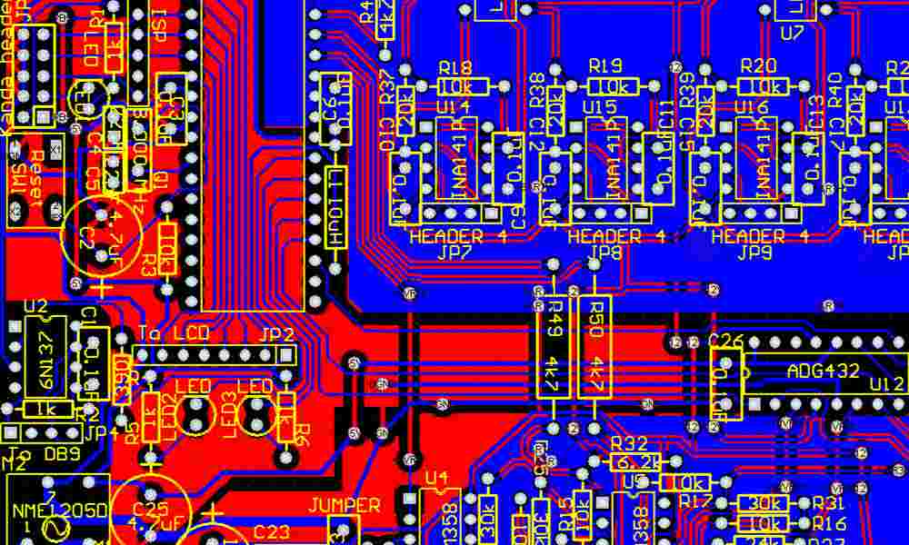
Layers
You can learn to slice every feature in individual layers. A physical board comprises several layers of various materials bonded through various processes. Separate design layers make up these material layers. KiCad displays these layers on the right side. Also, copper layers are on the top and other layers follow.
Footprints
A PCB footprint editor helps to create footprints in KiCad. Also, components can either come in non-standard packages or standard ones. For instance, an 8 pin DIP with a width of 7.62mm is a standard Integrated circuit package. Any integrated circuit (IC) that has the standard package dimensions will match with a standard footprint. Also, the footprint library in KiCad comprises thousands of standard footprints.
Therefore, you don’t need to worry about creating all the footprints yourself. However, if you can’t find the footprint for a component in the libraries, you can create on for yourself. Alternatively, search for an already-created one on the internet.
Generally, there are two major types of footprints. These are surface mount and through-hole. It is crucial to know the discrepancies between these two footprints.
Surface mount footprint
Surface mount technology (SMT) enables component placement and soldering on any side of the circuit board while maximizing space. Also, this technology is popularly used in today’s world. Surface mount devices (SMD) are components integrated by SMT. Surface mount has more benefits than THT. Therefore, this makes it a highly preferred technology for mass production of electronic products.
Furthermore, THT components are bigger than SMT components. Therefore, SMT saves space when used in PCB manufacturing. It allows PCB manufacturers to fabricate more compact and complex boards. Due to its save spacing benefits, the size of the circuit board reduces.
THT footprint
Through hole technology (THT) components are usually inserted via holes on the circuit board. Also, these components feature leads that are very long. You can trim these leads after soldering. THT components offer several benefits. They create more bond between components. Also, they are very easy to disassemble and assemble on a printed circuit board. THT components are ideal for prototyping with breadboards.
How to Route in kiCad
Routing involves the drawing of tracks on the top copper layer. When copper layers have tracks, the PCB designer has routed the circuit. In PCB design, there are two ways of routing; manual or automatic.
EDA software integrates some algorithms to locate an optimized PCB layout in automatic routing. Furthermore, during this process, the autorouter can use jumpers or vias. This may yield a perfect outcome, where all tracks will route. Sometimes, you will need to route some tracks manually.
Automatic routing helps to quickly route prototype printed circuit board where positions and lengths aren’t crucial. However, you will need to use manual routing when you need control over a crucial design.
To route a circuit board, you must import the footprints to the board editor. We are yet to add the board outline. You can include a board outline by selecting layer, setting the grid, and drawing a rectangle all over the footprints. Also, the board outline is located on the Edge.Cuts layer. Draw the board outline with any shape tools or arc tools.
Frequently Asked Questions
What does the Footprint Assignment Tool do?
Once you have completed a schematic drawing, you can then create a layout printed circuit board. In a PCB design, all types of scales and measurements matter. PCB Editors have mechanical or physical constraints. Schematic symbols should have footprints to help convert the schematic to a circuit board. The footprint assignment tool comprises schematic symbol footprint filter i
Also, footprints have two dimensional physical layouts where the actual component can be soldered. For instance, a 5mm LED requires a footprint with two pads and two holes on the circuit.
You will see a new window with three columns anytime you open a footprint assignment tool. Also, the first column comprises collections of footprints. A library can feature several individual footprints. It is important we locate a footprint and assign it to symbols in the schematic.
How do you Update PCB from Schematic?
You can export any alterations from the PCB editor to the schematic editor. To do this, click on Tools and choose update schematic from PCB. For instance, you can change the value of the footprint assignment. Also, you can maintain parity by syncing such changes to the schematic sheet.
Conclusion
KiCad is capable of creating all the essential files needed for developing circuit boards. These files include drilling files, component location files, and Gerber files for photo-plotters. Also, KiCad tutorial is suitable for the creation of electronic hardware. In this KiCad tutorial, we have explained how to use this software and everything it entails.
