Power printed circuit board (PCB) design plays a pivotal role in the development of electronic devices, as it helps in optimizing the performance and functionality of the equipment. As a beginner in this field, understanding the fundamental aspects of power PCB design is essential for ensuring the longevity and effectiveness of the electronic devices. In this article, we will discuss five major things newcomers to power PCB design need to know in order to create efficient and reliable designs.
Selecting the right materials, understanding the relationship between trace widths and current carrying capacity, and component placement can significantly impact your power PCB design. By taking these factors into consideration, along with thermal management, you can improve the overall performance and reliability of your electronic devices.
In addition to these ameliorations, being aware of the potential design challenges and addressing them from the onset can make an enormous difference in the success of your power PCB project. This knowledge will equip you with a skill set that will ultimately lead to practical and effective design solutions. As you progress in the field of power PCB design, applying these fundamental principles will only enhance your abilities and increase your confidence as a designer.
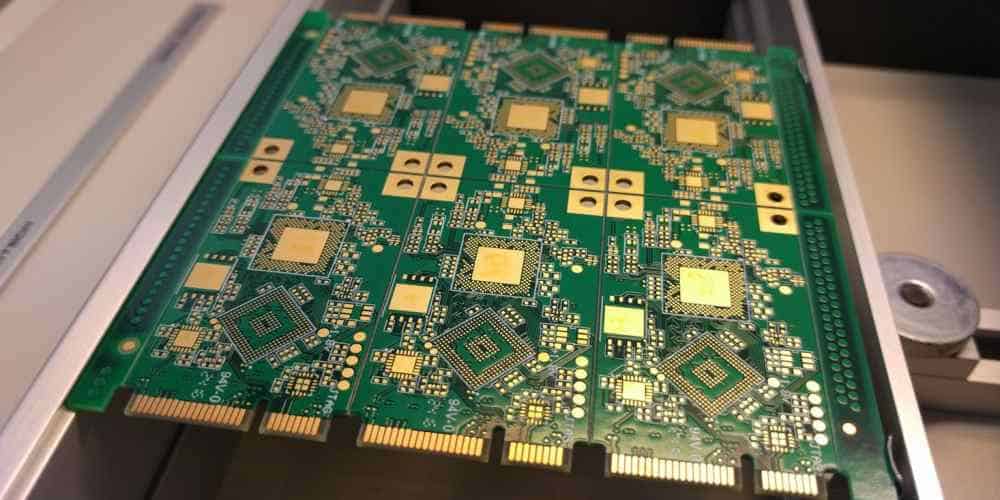
Power PCB Fundamentals
Definition and Purpose
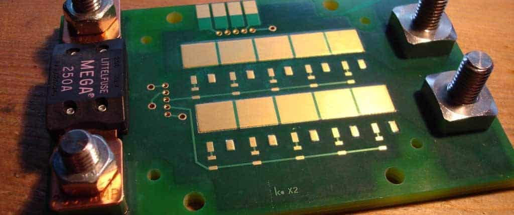
A Power Printed Circuit Board (PCB) is a board specifically designed to handle a higher level of current and voltage compared to a regular PCB. The primary purpose of a Power PCB is to distribute power efficiently among various components of a circuit, thus enhancing the stability and performance of electronic devices.
Power PCBs play a critical role in a wide range of applications, ranging from industrial equipment to consumer electronics. They are commonly found in power converters, power amplifiers, and high current applications.
Materials and Layers
Materials and layers are the two major components that significantly contribute to the efficiency and durability of Power PCBs.
-
Materials: High-quality materials ensure adequate heat dissipation and robust performance in power PCBs. The most common material used for the substrate is FR4, which is known for its excellent mechanical and thermal properties. Sometimes, metal core PCBs (MCPCBs) with aluminum or copper cores are utilized for better thermal management.
-
Layers: The number of layers in a PCB affects the design complexity and the amount of current it can handle. Power PCBs can have single-layer, double-layer, or multi-layer configurations, depending on the application requirements. Multi-layer designs offer better noise reduction and signal integrity due to the possibility of incorporating dedicated power and ground planes.
It is crucial to understand the fundamentals of materials and layers when designing a Power PCB to achieve optimal functionality and reliability in the final product.
Design Considerations
Power Handling and Distribution
When designing a power PCB, it is crucial to consider how much power the board needs to handle and ensure proper distribution to all components. This can be achieved by:
- Calculating the total power required by the components
- Selecting appropriate power sources, such as AC/DC or switching regulators
- Designing power distribution network (PDN) and allocating sufficient copper area to handle current flow
Thermal Management
Managing heat generated by components and power circuits is essential to maintain the reliability and performance of the board. Some considerations for thermal management include:
- Identifying and placing high-heat-producing components strategically
- Utilizing heat sinks or thermal vias to dissipate heat
- Designing proper cooling mechanisms, such as airflow or active cooling
Ground Planes
A ground plane is a large copper area used as a common reference point for electrical signals. Ground planes are crucial for achieving a stable and noise-free operation. Some ground plane considerations include:
- Providing a continuous and uniform ground plane for optimal signal return path
- Separating digital and analog ground planes to minimize noise coupling
- Adding ground stitching vias to connect different ground layers
Trace Design
Traces carry electrical signals between components on a PCB. The design and layout of these traces affect the overall performance of the circuit. Some factors to consider for trace design include:
- Calculating trace dimensions based on the desired impedance and current carrying capability
- Minimizing the length of signal traces to reduce noise and crosstalk
- Using differential pairs and proper routing techniques to optimize signal integrity
Design Tools and Techniques

CAD Software
Computer-aided design (CAD) software is essential for creating power PCB designs. Some popular CAD software options for PCB design include:
It’s crucial for beginners to pick a user-friendly CAD software that suits their requirements and budget. To select the best software, consider the following aspects:
- Ease of use and learning curve
- Capability to handle complex designs
- Available libraries and components
- License fees and support
Once a suitable CAD software is chosen, it’s important to learn its features, including schematic capture, PCB layout, and design rule checking.
Design for Manufacturability
Design for manufacturability (DFM) ensures that the PCB design can be efficiently produced at scale. This involves considerations to prevent potential manufacturing problems, reduce production costs, and improve the overall quality. Here are some key points for DFM:
-
Component Selection: Choose widely available and reliable components. Avoid using outdated or hard-to-source parts.
-
Spacing and Placement: Ensure adequate spacing between components to prevent interference or overheating. Place related components close together to minimize trace lengths and reduce signal noise.
-
Routing and Vias: Use a minimum trace width as recommended by the manufacturer, and limit the number of vias to keep production costs low.
-
Design Rule Check (DRC): Run a DRC to detect any potential errors or violations in your design. Most CAD software tools provide built-in DRC functions.
Remember to consult the PCB manufacturer’s guidelines and ensure your design adheres to their specifications.
Testing and Debugging
Simulation Tools
Simulation tools are essential in the PCB design process as they allow you to identify potential issues before prototyping. These tools analyze the electrical performance and compatibility of components within your design. Some popular simulation tools include:
- LTspice
- PSpice
- Multisim
Using the right simulation tool can help you identify potential issues and prevent unexpected problems during the prototyping process.
PCB Prototyping
Once your design is ready, prototyping helps verify its functionality by fabricating a physical test board. This stage can reveal issues that may not have been apparent in the simulation or design review. Some common PCB prototyping methods include:
- Breadboarding
- Laser cutting
- CNC milling
Selecting the appropriate prototyping method depends on the complexity of your design and the materials required.
Design Review and Validation
An essential part of the testing and debugging process is reviewing your design to find errors and inconsistencies. This can involve:
- Checking for missing components
- Verifying connections and traces
- Ensuring clearances and tolerances are met
In addition to self-review, an experienced professional or peer review can offer valuable insight and help identify potential problems.
Validation is carried out after the prototype has been successfully tested. This ensures your final design meets the specified requirements and is ready for mass production.
