PCB practical is an essential aspect of modern electronics. PCB, which stands for Printed Circuit Board, is a board made of insulating material and a conductive layer that connects electronic components. PCBs are used in almost all electronic devices, from smartphones to computers to cars. They are essential in providing a stable and reliable connection between electronic components.
In this article, we will explore the basics of PCB practical. We will discuss the different types of PCBs, the materials used in PCB manufacturing, and the manufacturing process. We will also delve into the advantages of using PCBs in electronic devices, including their durability, reliability, and cost-effectiveness. Whether you are a beginner in electronics or an experienced engineer, this article will provide you with a comprehensive understanding of PCB practical.
PCB Practical Basics
What is a PCB?
A Printed Circuit Board (PCB) is a board made of insulating material, such as fiberglass or plastic, with conductive pathways etched onto its surface. These pathways are used to connect electronic components, such as resistors, capacitors, and microchips, to create a functioning electronic circuit.
Types of PCBs
There are several types of PCBs, including single-layer, double-layer, and multi-layer PCBs. Single-layer PCBs are the simplest and most affordable type, with all the components mounted on one side of the board. Double-layer PCBs have components mounted on both sides of the board, and the conductive pathways run through the board to connect them. Multi-layer PCBs are the most complex type, with several layers of conductive pathways sandwiched between insulating layers.
PCB Design Basics
Designing a PCB involves several steps, including schematic capture, component placement, and routing. Schematic capture involves creating a diagram of the circuit to be built, showing the components and their connections. Component placement involves arranging the components on the board in a way that minimizes the length of the conductive pathways. Routing involves drawing the conductive pathways on the board to connect the components according to the schematic.
When designing a PCB, it’s important to consider factors such as the size of the board, the number of components, and the power requirements of the circuit. It’s also important to follow best practices for PCB design, such as keeping conductive pathways as short as possible, avoiding sharp angles, and providing adequate clearance between components.
In conclusion, understanding the basics of PCB design is crucial for anyone working with electronics. By following best practices and considering the specific requirements of each circuit, it’s possible to create reliable and efficient PCBs for a wide range of applications.
PCB Fabrication

Overview of PCB Fabrication Process
PCB fabrication is the process of creating printed circuit boards (PCBs) that are used to connect electronic components. The process involves several steps, including designing the PCB layout, selecting the appropriate materials, and etching the PCB.
PCB Material Selection
The choice of PCB material is crucial in determining the overall performance and reliability of the PCB. The most commonly used materials for PCBs are FR-4 (fiberglass reinforced epoxy laminate), polyimide, and aluminum. FR-4 is the most widely used material due to its low cost and high performance. Polyimide is used in high-temperature applications, while aluminum is used in high-power applications.
PCB Layer Stackup
The PCB layer stackup refers to the arrangement of copper layers and insulating layers in a PCB. The number of layers in a PCB can range from 1 to 30 or more, depending on the complexity of the design. The layer stackup plays a crucial role in determining the impedance, signal integrity, and power distribution of the PCB.
PCB Etching Process
The PCB etching process involves removing unwanted copper from the PCB using a chemical solution. The process begins with the application of a photoresist to the copper layer. The photoresist is then exposed to UV light, which hardens the areas that will remain after etching. The PCB is then placed in an etching solution that removes the unwanted copper. Finally, the remaining photoresist is removed, leaving behind the desired copper traces.
Overall, PCB fabrication is a complex process that requires careful attention to detail and a deep understanding of the materials and processes involved. By following the proper procedures and selecting the appropriate materials, designers can create high-performance and reliable PCBs for a wide range of applications.
PCB Assembly
Overview of PCB Assembly Process
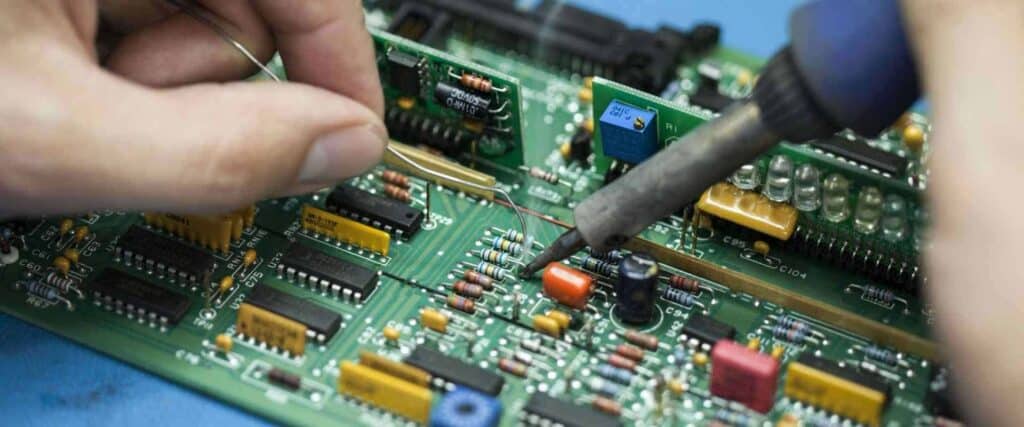
PCB assembly, also known as PCBA, is the process of assembling electronic components onto a printed circuit board (PCB). The process involves several steps, including soldering components onto the board, testing the board for functionality, and inspecting the board for any defects.
The PCB assembly process starts with the preparation of the board, which involves cleaning and coating the board with a layer of solder paste. The components are then placed onto the board using a pick-and-place machine, and the board is placed into a reflow oven to melt the solder paste and secure the components onto the board.
PCB Assembly Techniques
There are two main techniques used in PCB assembly: through-hole and surface mount technology (SMT). Through-hole technology involves drilling holes in the board and inserting components through the holes, while SMT involves placing components directly onto the surface of the board.
SMT is the most commonly used technique in modern PCB assembly due to its smaller size, higher component density, and faster assembly time. However, through-hole technology is still used in certain applications where a stronger mechanical connection is required.
Through-Hole vs Surface Mount Technology
Through-hole technology provides a stronger mechanical connection due to the component being inserted through the board and soldered on both sides, but it requires more space on the board and is slower to assemble. SMT components are smaller and can be placed closer together, allowing for a higher component density on the board and faster assembly time.
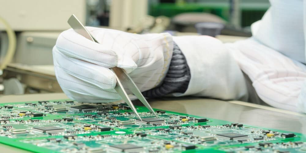
PCB Inspection and Testing
After the components have been assembled onto the board, the board is inspected for any defects or issues. This includes both visual inspection and functional testing to ensure that the board is working properly.
Visual inspection involves checking for any solder defects or misaligned components, while functional testing involves testing the board with a signal generator or other testing equipment to ensure that it is functioning as intended.
Overall, PCB assembly is a critical step in the production of electronic devices, and it requires careful attention to detail to ensure that the final product is of high quality and reliability.
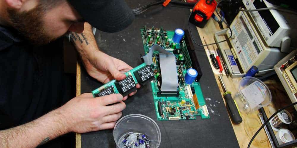
PCB Troubleshooting
Common PCB Issues
PCBs are prone to a range of issues that can occur during the manufacturing process or due to external factors. Here are some of the most common PCB issues:
- Short circuits: A short circuit occurs when two or more electrical signals come into contact with each other, causing an unintended flow of current. This can be caused by a variety of factors, including manufacturing defects, wiring errors, or component failures.
- Open circuits: An open circuit occurs when there is a break in the electrical connection, preventing current from flowing. This can be caused by a damaged trace, a disconnected component, or a faulty solder joint.
- Component failures: Components can fail due to a variety of factors, including manufacturing defects, environmental factors, or electrical overstress. Symptoms of component failure can include overheating, erratic behavior, or complete failure to function.
- Noise: Electrical noise can cause interference with the intended signals on a PCB, leading to signal degradation or complete failure. Sources of noise can include electromagnetic interference (EMI), radio frequency interference (RFI), or power supply noise.
Troubleshooting Techniques
When troubleshooting a PCB, it’s important to follow a systematic approach to isolate the issue and identify the root cause. Here are some common troubleshooting techniques:
- Visual inspection: A visual inspection of the PCB can often reveal obvious issues such as damaged traces, disconnected components, or obvious manufacturing defects. This can be done with the naked eye or with the aid of a microscope or magnifying glass.
- Electrical testing: Electrical testing can be used to measure the voltage, current, and resistance of various components and traces on the PCB. This can help identify issues such as short circuits, open circuits, or faulty components.
- Signal tracing: Signal tracing involves following the path of a signal through the PCB to identify where it is being lost or degraded. This can be done with the aid of an oscilloscope or logic analyzer to visualize the signal and identify any anomalies.
- Component substitution: Component substitution involves replacing suspect components with known good ones to see if the issue is resolved. This can help isolate the root cause of the issue and identify faulty components.
By following a systematic approach to PCB troubleshooting, it’s possible to identify and resolve a wide range of issues that can occur during the manufacturing process or during the life of the PCB.
