Printed circuit boards (PCBs) are the backbone of the electronics industry. They are used in almost every electronic device, from smartphones to industrial machinery. PCBs are made by printing conductive pathways onto a non-conductive substrate, which allows for the flow of electrical current.
The process of PCB production involves several steps, including design, printing, etching, drilling, and assembly. Design involves creating a schematic of the circuit and laying out the components on the board. Printing involves transferring the design onto the substrate using a special ink or toner. Etching involves removing the unwanted copper from the board using a chemical process. Drilling involves creating holes for the components to be inserted, and assembly involves attaching the components to the board.
PCB production has come a long way since its inception in the 1940s. With the advent of computer-aided design (CAD) and automated assembly, the process has become faster, more precise, and more efficient. As a result, PCBs are now more affordable and accessible than ever before, making them an essential component of modern technology.

Basics of Printed Circuit Board Production
Designing the PCB
Printed Circuit Board (PCB) production starts with designing the PCB. The design process involves creating a schematic diagram of the circuit and laying out the components on the board. The design software is used to create the schematic diagram and layout design. The software allows designers to check for errors and optimize the design before manufacturing.
Manufacturing the PCB
Once the design is complete, the manufacturing process starts. The manufacturing process involves several steps, including:
- Printing: The design is printed onto a copper-clad board using a photosensitive material. The photosensitive material is exposed to UV light, which hardens the areas that will be etched away.
- Etching: The board is then etched using a chemical solution that removes the copper from the areas that were not hardened by the UV light. This leaves behind the copper traces that make up the circuit.
- Drilling: Holes are drilled into the board where components will be placed. The holes are then plated with copper to create electrical connections between the layers of the board.
- Soldering: Components are then soldered onto the board using a soldering iron or reflow oven. The components are placed in the holes and soldered to the copper traces on the board.
PCB production is a complex process that requires expertise and precision. PCBs are used in a wide range of electronic devices, from smartphones to industrial equipment. Understanding the basics of PCB production is essential for anyone involved in electronics design and manufacturing.
Types of Printed Circuit Boards
Printed Circuit Boards (PCBs) come in different types, each with its own distinct characteristics. Here are the three main types of PCBs:
Single-Sided PCBs
Single-sided PCBs are the simplest type of PCBs, with components mounted on one side of the board and the copper tracks on the other. They are used for low-cost, low-density applications and are ideal for simple circuits.
Single-sided PCBs are easy to manufacture and are often used in toys, calculators, and other low-cost electronic devices. They are also used in industries such as automotive, aerospace, and medical.
Double-Sided PCBs
Double-sided PCBs have components mounted on both sides of the board, with copper tracks on both sides as well. They are used for more complex circuits and higher density applications.
Double-sided PCBs are more difficult to manufacture than single-sided PCBs, but they offer more flexibility in terms of design. They are used in a wide range of applications, including telecommunications, industrial control systems, and consumer electronics.
Multi-Layer PCBs
Multi-layer PCBs have more than two layers of copper tracks sandwiched between insulating layers. They are used for very complex circuits and high-density applications.
Multi-layer PCBs are more expensive to manufacture than single-sided and double-sided PCBs, but they offer many advantages. They allow for more complex designs, reduce electromagnetic interference, and can handle higher frequencies. They are used in applications such as high-speed data processing, aerospace, and military systems.
In conclusion, understanding the different types of PCBs is essential when designing electronic circuits. Each type of PCB has its own unique characteristics, and choosing the right one for your application is crucial for the success of your project.
Materials Used in PCB Production

Substrates
The substrate is the base material upon which the printed circuit board is built. The most commonly used materials for substrates are fiberglass-reinforced epoxy resin (FR-4) and polyimide. FR-4 is a composite material made of woven fiberglass cloth and epoxy resin, and it is widely used because of its excellent electrical insulation properties, high strength, and low cost. Polyimide, on the other hand, is a high-temperature plastic that is used in applications where the board will be exposed to high temperatures.
Conductive Materials
The conductive materials used in PCB production are copper and aluminum. Copper is the most commonly used material for conductive traces on printed circuit boards because of its high conductivity, low cost, and ease of use. Aluminum is used in some specialized applications where weight is a concern, such as in aerospace and military applications.
Solder Masks
Solder masks are used to protect the copper traces on the PCB from accidental soldering during assembly. They are typically made of a polymer material and applied to the board using a silk-screening process. Solder masks are available in a variety of colors, with green being the most commonly used color.
Legend Inks
Legend inks are used to print identifying information on the surface of the PCB, such as component designators, logos, and other markings. They are typically applied using a silk-screening process and are available in a variety of colors, with white being the most commonly used color.
In summary, the materials used in PCB production include substrates, conductive materials, solder masks, and legend inks. These materials are carefully selected based on their properties and the specific requirements of the PCB being produced.
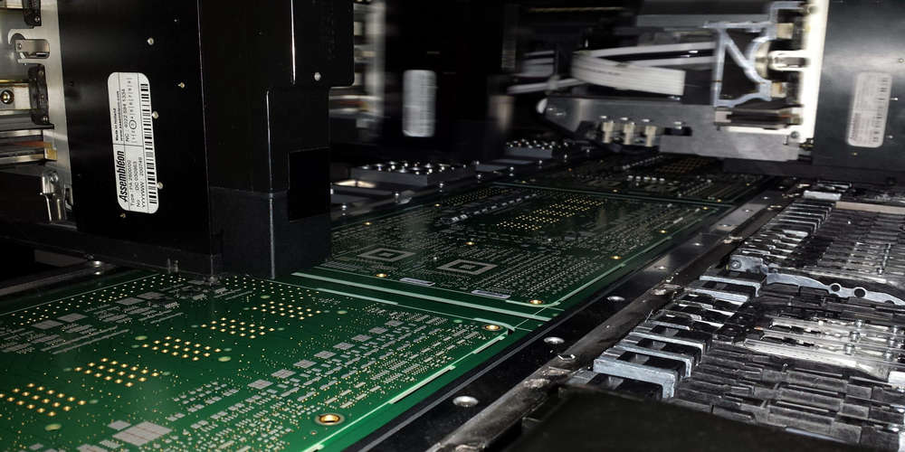
PCB Assembly
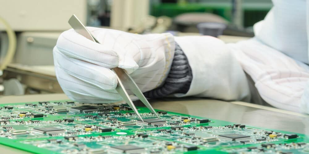
When it comes to printed circuit board (PCB) production, assembly is a crucial step in the process. PCB assembly involves attaching electronic components to the board, which can be done through two methods: Through-Hole Assembly and Surface Mount Technology (SMT).
Through-Hole Assembly
Through-Hole Assembly is an older method of PCB assembly that involves drilling holes through the board and inserting components through the holes. The components are then soldered onto the board from the other side. Through-Hole Assembly is known for its durability and reliability, making it a popular choice for applications that require high levels of vibration or shock resistance.
However, Through-Hole Assembly has some downsides. It is more time-consuming and expensive than SMT, and it requires more space on the board. Additionally, Through-Hole Assembly is not suitable for small components, as the holes must be large enough to accommodate the leads.
Surface Mount Technology
Surface Mount Technology (SMT) is a newer method of PCB assembly that involves attaching components directly to the surface of the board. SMT components are smaller and lighter than Through-Hole components, making them ideal for applications where space is limited.
SMT is also faster and less expensive than Through-Hole Assembly, as it does not require drilling holes through the board. However, SMT components are more fragile than Through-Hole components, making them more susceptible to damage from vibration or shock.
In conclusion, both Through-Hole Assembly and Surface Mount Technology have their advantages and disadvantages. The choice between them depends on the specific needs of the application.
Quality Control in PCB Production
Quality control is an essential part of the printed circuit board production process. It ensures that the PCBs meet the required standards and specifications, and that they function correctly. Quality control measures are implemented throughout the production process to minimize the risk of defects and ensure that the final product is of high quality.
One of the primary quality control measures in PCB production is the inspection of the raw materials. The quality of the materials used in the production process can have a significant impact on the final product’s quality. Therefore, it is crucial to ensure that the materials meet the required standards and specifications before they are used in the production process.
Another critical quality control measure is the inspection of the PCBs during and after the production process. This includes visual inspection, electrical testing, and functional testing. Visual inspection is used to check for any defects, such as cracks, scratches, or other physical damage. Electrical testing is used to check for any electrical faults, such as open circuits or short circuits. Functional testing is used to check that the PCBs meet the required specifications and perform as expected.
In addition to these measures, quality control also involves monitoring and controlling the production process itself. This includes controlling the temperature and humidity levels, ensuring that the equipment is calibrated correctly, and that the production process is carried out according to the required standards and specifications.
Overall, quality control is an essential part of PCB production. It ensures that the final product is of high quality, meets the required specifications, and functions correctly. By implementing quality control measures throughout the production process, manufacturers can minimize the risk of defects and ensure that their products are of the highest quality.
Future of PCB Production
As technology advances, so does the production of printed circuit boards (PCBs). In the future, PCB production is expected to become even more efficient and cost-effective. Here are some of the trends that are likely to shape the future of PCB production:
-
Miniaturization: PCBs are becoming smaller and more compact, which means that manufacturers will need to use more advanced techniques to produce them. This trend is driven by the need for smaller and more powerful electronic devices.
-
Automation: As with many other industries, PCB production is becoming increasingly automated. This trend is driven by the need to reduce costs and improve efficiency. Automated production lines can produce PCBs faster and with greater accuracy than manual processes.
-
Flexible PCBs: Flexible PCBs are becoming more popular, particularly in the medical and wearable technology industries. These PCBs can be bent and shaped to fit into tight spaces, making them ideal for use in small and portable devices.
-
Smart PCBs: Smart PCBs are PCBs that have built-in sensors and other electronic components. These PCBs are becoming more common in the Internet of Things (IoT) industry, where they can be used to collect and transmit data from a variety of sources.
-
Eco-friendly production: As consumers become more environmentally conscious, manufacturers are looking for ways to produce PCBs in a more sustainable way. This includes using eco-friendly materials and reducing waste during the production process.
Overall, the future of PCB production looks bright. With advancements in technology and a focus on efficiency and sustainability, manufacturers are well-positioned to meet the growing demand for PCBs in a variety of industries.
