Printed circuit design and fabrication is a critical aspect of modern electronics manufacturing. It involves the creation of custom circuit boards that are essential components of electronic devices. The process of designing and fabricating a printed circuit board involves several steps, including schematic capture, board layout, manufacturing, and testing.
The design phase of printed circuit board fabrication involves creating a schematic of the circuit and laying out the board’s components. This step is crucial because it determines the board’s functionality and performance. The schematic captures the electrical connections between the components, while the board layout determines the physical arrangement of the components on the board. Once the design is complete, the board is manufactured using a variety of techniques, including etching, drilling, and plating. Finally, the board is tested to ensure that it meets the required specifications.
The Importance of Printed Circuit Design and Fab
Printed circuit design and fabrication are essential processes in the production of electronic devices. The design and fabrication of printed circuit boards (PCBs) are critical to the proper functioning of electronic devices. A poorly designed or fabricated PCB can lead to unreliable products, increased costs, and even safety hazards.
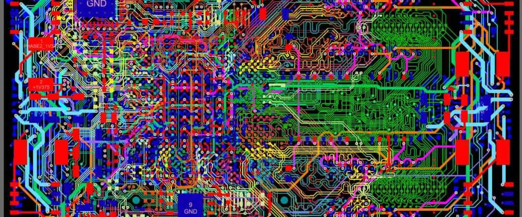
The design of a PCB involves the placement of components and the routing of electrical connections. A well-designed PCB should minimize interference between components, reduce signal loss, and ensure that the circuit operates as intended. A poorly designed PCB can lead to signal degradation, crosstalk, and other issues that can affect the performance of the circuit.
The fabrication of a PCB involves the actual production of the board itself. The process includes the creation of the copper traces, the drilling of holes, and the application of solder mask and silkscreen. The quality of the fabrication process can affect the reliability and durability of the PCB. A poorly fabricated PCB can have issues such as delamination, poor adhesion, and warping.
In conclusion, the importance of printed circuit design and fabrication cannot be overstated. A well-designed and fabricated PCB is essential to the proper functioning of electronic devices. It is crucial to work with experienced and knowledgeable PCB designers and fabricators to ensure that your PCBs meet the necessary standards and specifications.
Key Considerations for Printed Circuit Design and Fab

Printed circuit boards (PCBs) are an essential component of electronic devices. They provide a platform for connecting electronic components, and their design and fabrication are critical for the overall performance of the device. Here are some key considerations for printed circuit design and fab:
PCB Design Considerations
-
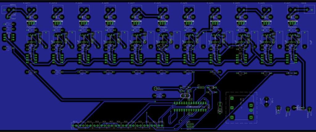
Component Placement: Component placement is crucial for the performance of the device. Proper placement can reduce noise, improve signal integrity, and minimize crosstalk. It is essential to consider the placement of components, their orientation, and their proximity to each other.
-
Trace Routing: Trace routing is the process of connecting components on the PCB. It is essential to ensure that the traces are of the right width, length, and spacing to avoid signal distortion, crosstalk, and noise.
-
Layer Stackup: The layer stackup determines the number of layers in the PCB and their arrangement. It is crucial to select the right layer stackup to meet the design requirements, reduce noise, and improve signal integrity.
PCB Fabrication Considerations
-
Substrate Material: The substrate material is the base material used to make the PCB. It is essential to select the right substrate material based on the design requirements, the operating environment, and the manufacturing process.
-
Copper Thickness: Copper thickness is an important factor that affects the performance of the PCB. It is essential to select the right copper thickness to meet the design requirements, reduce noise, and improve signal integrity.
-
Plating and Coating: Plating and coating are essential processes used to protect the PCB from environmental factors such as moisture, corrosion, and oxidation. It is crucial to select the right plating and coating materials and processes to meet the design requirements and the operating environment.
In conclusion, the design and fabrication of printed circuit boards are critical for the overall performance of electronic devices. Proper consideration of the above factors can help ensure that the PCB meets the design requirements, reduces noise, improves signal integrity, and performs optimally in the operating environment.
The Printed Circuit Design Process
The printed circuit design process is a critical part of creating electronic devices. It involves designing the layout of the circuit board, selecting the appropriate components, and creating the necessary files for fabrication. Here are the steps involved in the printed circuit design process:
-
Schematic Design: The first step in the printed circuit design process is creating a schematic diagram. This diagram shows the components and connections of the circuit. It is essential to ensure that the design meets the requirements and specifications of the device.
-
Component Selection: Once the schematic is complete, the next step is to select the appropriate components. This involves choosing the right type of components, such as resistors, capacitors, and integrated circuits, and ensuring that they meet the requirements of the design.
-
PCB Layout Design: After selecting the components, the next step is to create the PCB layout design. This step involves placing the components on the board and routing the connections between them. It is essential to ensure that the layout is optimized for performance, manufacturability, and reliability.
-
Design Verification: Once the PCB layout is complete, the next step is to verify the design. This involves checking for errors, such as incorrect connections, missing components, and design rule violations. It is essential to ensure that the design is error-free before moving on to the fabrication stage.
-
File Generation: After verifying the design, the next step is to generate the necessary files for fabrication. This involves creating the Gerber files, drill files, and other files required by the manufacturer. It is essential to ensure that the files are generated correctly and that they meet the manufacturer’s requirements.
In conclusion, the printed circuit design process is a critical part of creating electronic devices. It involves designing the layout of the circuit board, selecting the appropriate components, and creating the necessary files for fabrication. By following the steps outlined above, designers can create high-quality printed circuit boards that meet the requirements and specifications of the device.
The Printed Circuit Fabrication Process
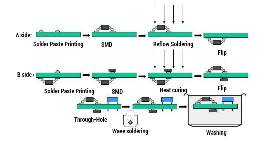
Printed circuit boards (PCBs) are the foundation of modern electronics. They are used in everything from smartphones and laptops to cars and airplanes. PCBs are made up of layers of copper and other materials that are etched to create a circuit pattern. The fabrication process involves several steps, including design, imaging, etching, drilling, and plating.
Design
The first step in the PCB fabrication process is design. The circuit board is designed using software such as Altium Designer or Eagle CAD. The design includes the layout of all the components, the routing of the traces, and the placement of the vias and pads.
Imaging
Once the design is complete, it is printed onto a special film called a photomask. The photomask is then used to transfer the design onto a copper-clad board using a process called photolithography. The board is coated with a light-sensitive material, and the photomask is placed on top. The board is then exposed to UV light, which hardens the material in the areas not covered by the photomask.
Etching
After the board has been imaged, it is etched to remove the copper in the areas not covered by the hardened material. The etching process uses a chemical solution to dissolve the copper, leaving behind the circuit pattern. Once the etching is complete, the board is cleaned and inspected for any defects.
Drilling
Next, the board is drilled to create holes for the vias and component leads. The holes are drilled using a CNC machine, which ensures precision and accuracy. Once the holes are drilled, the board is cleaned again to remove any debris.
Plating
The final step in the PCB fabrication process is plating. The board is plated with a thin layer of copper to protect the traces and provide a surface for soldering. The plating process involves immersing the board in a chemical solution and applying an electrical current. Once the plating is complete, the board is cleaned and inspected for any defects.
In conclusion, the PCB fabrication process is a complex and precise process that involves several steps. From design to plating, each step is critical to ensuring the final product is of high quality and meets the required specifications.
Common Issues in Printed Circuit Design and Fab
Printed circuit design and fab are critical processes in the electronics industry. However, they are not without their challenges. Here are some common issues that designers and manufacturers encounter:
-
Design errors: One of the most common issues in printed circuit design is errors in the design. This can be due to a lack of attention to detail, lack of knowledge or experience, or miscommunication between the designer and manufacturer. These errors can lead to costly rework, delays, and even product failure.
-
Component placement: Another issue that designers face is component placement. Poor component placement can lead to signal integrity issues, overheating, and other problems. It is important to consider the placement of components carefully and ensure that they are placed in the optimal location.
-
Trace routing: Trace routing is another critical aspect of printed circuit design. Poorly routed traces can lead to signal integrity issues, crosstalk, and other problems. It is important to ensure that traces are routed correctly and that they are not too close to each other.
-
Manufacturing defects: In the manufacturing process, defects can occur due to a variety of reasons, such as poor quality control, incorrect tooling, or operator error. These defects can lead to product failure, and it is important to catch them early on in the manufacturing process.
-
Material selection: Choosing the right materials for the printed circuit board is critical. Poor material selection can lead to issues such as thermal expansion, warping, and other problems. It is important to consider the properties of the materials carefully and choose the right materials for the job.
In conclusion, printed circuit design and fab are complex processes that require careful attention to detail to ensure success. By addressing these common issues, designers and manufacturers can create high-quality products that meet the needs of their customers.
Best Practices for Printed Circuit Design and Fab

Printed circuit design and fab are critical components of modern electronics manufacturing. A well-designed printed circuit board (PCB) can make all the difference in the performance and reliability of a product. Here are some best practices to follow when designing and fabricating PCBs:
-
Design for manufacturability (DFM): Consider the manufacturing process when designing a PCB. DFM involves designing a PCB that can be manufactured efficiently and cost-effectively. This includes factors such as the size and shape of the board, the placement of components, and the number of layers.
-
Use the right software: Choose the right software for PCB design. There are many options available, each with its own strengths and weaknesses. Some popular software options include Eagle PCB, Altium Designer, and KiCad.
-
Follow design rules: Follow design rules to ensure that the PCB is manufacturable and reliable. Design rules include minimum trace widths, minimum clearance between traces, and minimum drill sizes.
-
Choose the right materials: Choose the right materials for the PCB. The choice of materials can affect the performance and reliability of the board. Common materials used in PCBs include FR-4 (fiberglass), polyimide, and Rogers.
-
Test the design: Test the design before fabrication. This can help identify any issues that may arise during manufacturing. Some common tests include design rule checks (DRC), electrical rule checks (ERC), and circuit simulation.
-
Choose the right manufacturer: Choose a manufacturer that can meet your requirements. Consider factors such as cost, lead time, and quality when selecting a manufacturer.
By following these best practices, you can ensure that your PCBs are manufacturable, reliable, and meet your requirements.
