Simple circuit PCB design is an essential aspect of electronics engineering. It involves designing and manufacturing printed circuit boards (PCBs) that are simple, effective, and efficient. PCBs are used in a wide range of electronic devices, including computers, smartphones, and televisions. They are also used in medical equipment, aerospace technology, and automotive systems.
The process of designing a simple circuit PCB involves several steps, including schematic capture, PCB layout, and PCB fabrication. Schematic capture involves creating a diagram of the circuit using specialized software. PCB layout involves placing the components on the board and routing the connections between them. PCB fabrication involves manufacturing the board using specialized equipment and materials.
Designing a simple circuit PCB requires a combination of technical knowledge, creativity, and attention to detail. Engineers must consider factors such as component placement, signal integrity, and thermal management. They must also ensure that the board meets industry standards and regulations. With the right skills and expertise, engineers can create simple circuit PCBs that are reliable, efficient, and cost-effective.
Basics of Simple Circuit PCB Design
When designing a simple circuit PCB, there are a few key considerations to keep in mind. Here are some basics to get you started:
-
Schematic design: Before you start designing your PCB, you’ll need to create a schematic diagram of your circuit. This will help you visualize the connections between components and ensure that everything is properly connected.
-
Component placement: Once you have your schematic, you’ll need to decide where to place your components on the PCB. This can have a big impact on the performance of your circuit, so it’s important to plan carefully. Consider factors like signal integrity, thermal management, and ease of assembly.
-
Trace routing: Once your components are placed, you’ll need to route the traces that connect them. This can be a complex process, especially if you’re dealing with high-speed signals or complex circuits. It’s important to pay attention to things like trace width, spacing, and impedance to ensure that your circuit will function properly.
-
Design rules: Most PCB design software will allow you to set up design rules that will help you ensure that your circuit meets certain standards. These rules can include things like minimum trace widths, maximum copper pours, and clearance distances. Setting up these rules early on can help you avoid costly mistakes down the line.
-
Testing and validation: Once your PCB is designed, it’s important to test and validate it thoroughly before sending it off for manufacturing. This can involve things like simulating your circuit in software, testing it on a breadboard, or using specialized testing equipment. By taking the time to test and validate your design, you can avoid costly mistakes and ensure that your circuit will work as intended.
By keeping these basics in mind, you can design simple circuit PCBs that are reliable, efficient, and easy to manufacture.
PCB Design Software

PCB design software is an essential tool for designing and creating printed circuit boards. It allows designers to create schematics, layout the board, and generate Gerber files for manufacturing. There are many PCB design software options available, each with its own strengths and weaknesses.
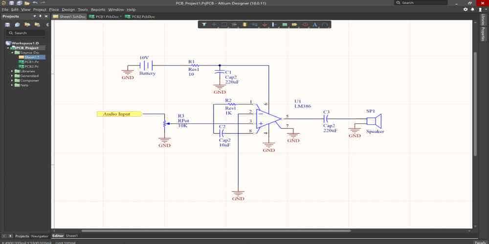
One popular option is Altium Designer, which offers a comprehensive suite of tools for schematic capture, PCB layout, and design rule checking. It also includes features for 3D visualization and collaboration with team members. However, it can be expensive and may have a steep learning curve for beginners.
Another option is Eagle PCB Design, which is known for its user-friendly interface and affordability. It offers a range of tools for schematic capture, board layout, and auto-routing. However, it may not be as powerful or feature-rich as other options.
KiCAD is a free, open-source option that has gained popularity in recent years. It offers a range of tools for schematic capture and PCB layout, as well as a 3D viewer and Gerber file generation. While it may not have all the features of paid options, it is continually improving and has a strong community of users.
No matter which PCB design software you choose, it is important to choose one that fits your specific needs and budget. It is also important to take the time to learn the software and become proficient in its use, as this can save time and prevent errors in the long run.
PCB Layout Design
PCB layout design is an essential step in the process of creating a simple circuit board. It involves arranging the components of the circuit board in a way that ensures proper functionality and efficient use of space. The following are some important aspects to consider when designing the PCB layout:
-
Component Placement: Component placement is crucial in ensuring that the circuit board functions as intended. It involves placing the components in a way that allows for proper connectivity and avoids signal interference.
-
Trace Routing: Trace routing involves creating pathways on the PCB that connect the different components. The routing should be done in a way that minimizes signal interference and ensures that the circuit board functions as intended.
-
Power and Ground Planes: Power and ground planes are an essential part of the PCB layout design. They provide a stable power and ground connection to the different components on the board and help reduce noise and interference.
-
Signal Integrity: Signal integrity is important in ensuring that the circuit board functions as intended. It involves ensuring that the signals transmitted on the board are not affected by noise or interference.
In conclusion, PCB layout design is an essential step in creating a simple circuit board. It involves careful consideration of component placement, trace routing, power and ground planes, and signal integrity. By following these guidelines, you can create a circuit board that functions as intended and is optimized for space and efficiency.
PCB Manufacturing Process
PCB manufacturing process involves several steps that transform the design into a physical circuit board. Here is a brief overview of the process:
-
Designing phase: In this phase, the PCB design is created using a software tool. The design includes the placement of components, routing of traces, and other specifications.
-
Printing phase: In this phase, the design is printed onto a copper-coated board using a special printer. This process is called “etching.”
-
Drilling phase: In this phase, the holes for components and vias are drilled into the board.
-
Plating phase: In this phase, a thin layer of metal is plated onto the holes and traces to create a conductive path.
-
Solder mask phase: In this phase, a layer of solder mask is applied over the board to protect it from oxidation and to make it easier to solder components onto the board.
-
Silkscreen phase: In this phase, a layer of ink is printed onto the board to label components and provide other information.
-
Testing phase: In this phase, the board is tested to ensure that it meets the required specifications.
Once the manufacturing process is complete, the PCB is ready for use. It can be installed in an electronic device and used to control the flow of electricity. With the right design and manufacturing process, a PCB can be a reliable and efficient component in any electronic device.
PCB Assembly Process

The PCB assembly process involves the creation of a printed circuit board (PCB) by soldering electronic components onto a board. The process is typically done using surface mount technology (SMT) or through-hole technology (THT).
Surface Mount Technology (SMT)
SMT is the most common method used for PCB assembly. It involves placing components directly onto the surface of the board and then soldering them in place. This method is faster and more cost-effective than THT.
The SMT process involves the following steps:
-
Stencil Printing: A stencil is used to apply solder paste to the board where the components will be placed.
-
Pick and Place: An automated machine places the components onto the board.
-
Reflow Soldering: The board is heated in a reflow oven, causing the solder paste to melt and bond the components to the board.
-
Inspection: The board is inspected to ensure that all components are properly soldered.
Through-Hole Technology (THT)
THT involves drilling holes into the board and inserting components through the holes. The components are then soldered to the board from the other side. This method is typically used for larger components or those that require a stronger bond.
The THT process involves the following steps:
-
Drilling: Holes are drilled into the board where the components will be inserted.
-
Component Insertion: The components are inserted into the holes.
-
Wave Soldering: The board is passed over a wave of molten solder, which bonds the components to the board.
-
Inspection: The board is inspected to ensure that all components are properly soldered.
Overall, the PCB assembly process is an important step in creating electronic devices. Whether using SMT or THT, it is essential to ensure that all components are properly soldered to the board to ensure the device functions correctly.
