PCB layout design is an essential aspect of electronics engineering. It involves designing the layout of a printed circuit board (PCB) to ensure that all the electronic components are correctly placed and connected. Simple PCB layout design is essential for beginners who are just starting with electronics engineering.
The process of designing a PCB layout can be challenging, but with the right tools and techniques, it can be made more manageable. One of the most critical aspects of simple PCB layout design is to ensure that all the components are correctly placed on the board. This involves understanding the electrical properties of each component and how they interact with each other. It is also important to ensure that the layout is optimized for the specific application to ensure that it performs as expected.
Another critical aspect of simple PCB layout design is to ensure that the board is easy to manufacture. This involves considering the manufacturing process when designing the layout. The board should be designed in a way that makes it easy to manufacture, assemble, and test. By following these guidelines, beginners can design simple PCB layouts that are functional, easy to manufacture, and optimized for their specific application.
Basics of PCB Layout Design
Design Considerations
When designing a PCB layout, it is important to consider the following factors:
-
Size and Shape: The size and shape of the PCB should be determined by the size and shape of the enclosure it will be housed in, as well as any other space constraints.
-
Number of Layers: The number of layers required for the PCB will depend on the complexity of the circuit and the number of components. A two-layer PCB is the most common, but more complex circuits may require four or more layers.
-
Trace Width and Spacing: The width and spacing of the traces should be determined by the current carrying capacity of the circuit and the voltage level. A wider trace can carry more current, while a narrower trace can save space.
-
Ground and Power Planes: Ground and power planes can help reduce noise and improve signal integrity. They should be placed on internal layers of the PCB.
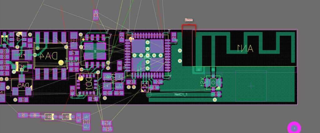
Component Placement
Component placement is a critical aspect of PCB layout design. The following guidelines should be considered:
-
Orientation: Components should be placed in a way that makes it easy to read their markings and identify their polarity.
-
Proximity: Components that interact with each other should be placed close together to minimize trace length and reduce noise.
-
Heat Dissipation: Components that generate heat, such as power transistors, should be placed in areas of the PCB that have good airflow or heat sinks.
-
Signal Flow: Components should be placed in a way that follows the signal flow of the circuit, from input to output.
By considering these design considerations and component placement guidelines, you can create a PCB layout that is functional, reliable, and efficient.
PCB Design Tools

When it comes to designing a PCB, having the right tools can make all the difference. There are a variety of software options available for PCB layout design, each with its own set of features and capabilities.
Software Options
Some popular software options for PCB layout design include Altium Designer, Eagle PCB, and KiCAD. Altium Designer is a professional-grade software with a wide range of features, but it comes with a higher price tag. Eagle PCB is a more affordable option with a user-friendly interface, but it has a more limited feature set. KiCAD is a free and open-source option that is gaining popularity for its versatility and community support.
Features and Capabilities
When choosing a PCB design tool, it’s important to consider the features and capabilities that are most important for your project. Some common features to look for include:
- Schematic capture: the ability to create a schematic diagram of your circuit
- Component libraries: pre-built libraries of commonly used components
- Auto-routing: the ability to automatically route traces on your PCB
- Design rule checking: the ability to check your design against specific rules and constraints
- 3D visualization: the ability to view your design in 3D and detect potential issues
In addition to these features, it’s important to consider the overall ease of use and compatibility with other tools and software in your workflow.
Overall, choosing the right PCB design tool can help streamline the design process and ensure a successful end result.
Designing for Manufacturability

When designing a PCB layout, it is important to consider manufacturability. This means that the design should be optimized for efficient and cost-effective production. Here are some key factors to keep in mind:
Layer Count
The number of layers in a PCB affects both the cost and complexity of manufacturing. More layers generally mean higher costs and longer lead times. Therefore, it is important to keep the layer count as low as possible while still achieving the necessary functionality. This can be achieved through careful component placement and routing.
Trace Width
The width of traces on a PCB affects both the electrical performance and manufacturability. Narrow traces are more difficult and expensive to manufacture, while wider traces can lead to signal integrity issues. It is important to find a balance between these factors when selecting trace widths. The table below provides some general guidelines for trace widths based on current carrying capacity:
| Current (A) | Trace Width (mil) |
|---|---|
| 0-0.5 | 5-10 |
| 0.5-1 | 10-20 |
| 1-3 | 20-30 |
| 3-5 | 30-40 |
| 5-8 | 40-50 |
| 8-10 | 50-60 |
Spacing
The spacing between traces and components on a PCB also affects manufacturability. Too little spacing can result in manufacturing defects such as shorts or solder bridges. Too much spacing can lead to unnecessarily large PCBs and increased costs. The table below provides some general guidelines for spacing between traces and components:
| Feature | Spacing (mil) |
|---|---|
| Trace-trace | 6-8 |
| Trace-pad | 8-10 |
| Pad-pad | 10-12 |
| Component-component | 12-14 |
| Component-edge | 20-24 |
By considering these factors when designing a PCB layout, you can optimize for manufacturability and achieve a high-quality, cost-effective product.
Advanced Techniques
Signal Integrity
Signal integrity is a critical aspect of PCB design. It refers to the ability of a circuit to transmit signals without distortion or loss. There are several techniques that can be used to ensure good signal integrity:
- Ground planes: Ground planes provide a low-impedance path for return currents, reducing noise and crosstalk.
- Signal routing: Signal traces should be kept as short and direct as possible, and should be routed away from noisy components and power planes.
- Termination: High-speed signals should be properly terminated to prevent reflections and signal degradation.
Power Distribution
Proper power distribution is essential for reliable circuit operation. Here are some techniques to ensure good power distribution:
- Decoupling capacitors: Decoupling capacitors should be placed as close as possible to each power pin to reduce noise and voltage spikes.
- Power planes: Power planes provide a low-impedance path for power distribution, reducing voltage drops and noise.
- Bypass capacitors: Bypass capacitors should be placed between power and ground planes to filter out high-frequency noise and spikes.
By implementing these advanced techniques, you can ensure good signal integrity and power distribution in your PCB designs.
