Most consumers often require market-ready printed circuit boards for diverse electronic applications. PCB products are a consequence of the PCB manufacturing and assembly process. While a key pillar to all electronic products, printed circuit board application areas can be diverse. They fit well in the slightest and simplest devices like calculators to more complex electronic equipment. Further, application areas range from consumer electronics, medical sector, military, aerospace, etc.
The key to quality printed circuit boards is an excellent design besides picking a top and suitable PCB manufacturing partner. However, the two hinge on a proper understanding of the manufacturing and assembly process. This article will focus on the intricacies of pcb manufacturing and assembly.
Printed Circuit Boards
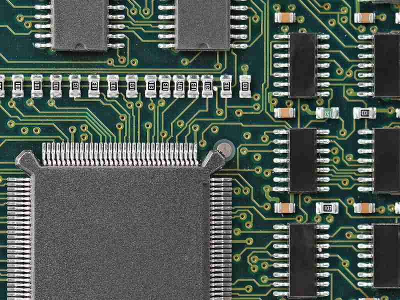
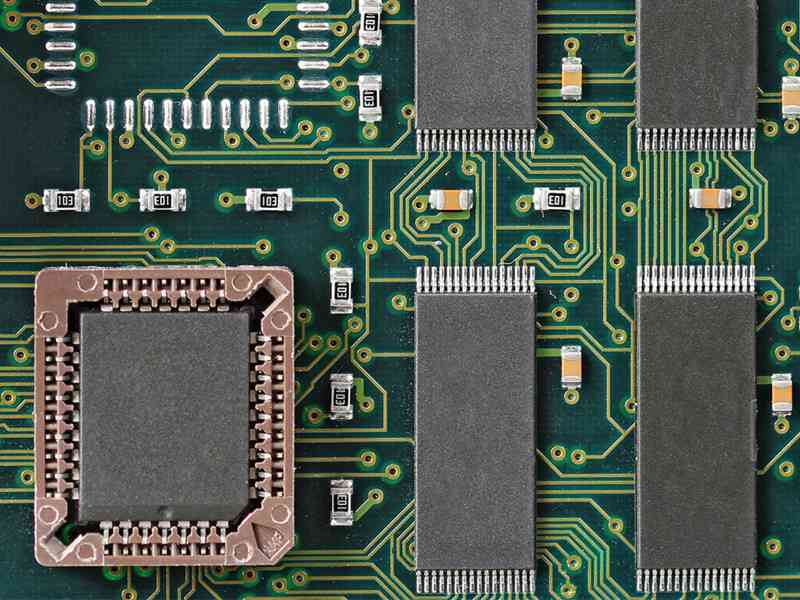
PCBs are instrumental in directing electrical and electronic signals in an electronic device or equipment. As a result, electronic products heavily rely on these PCBs. The global demand for electronic products has shot in recent years, cascading down to PCBs. For the uninitiated, printed circuit boards comprise conductive (copper layer) and non-conductive layers (substrate), all stacked together. It also has diverse components (both passive and active) that define its functionality.
PCBs are of varied types based on the number of stacked layers and the types of materials used in their fabrication. Additionally, the approach and technology used to design and fabricate it also define the type of PCB. For instance, design software technologies like KiCAD, Eagle, and Altium Designer can distinguish between printed circuit boards.
PCB Fabrication and Assembly
The production of printed circuit boards often combines PCB fabrication and assembly processes. As a PCB designer, understanding the various steps involved in the fabrication phase is crucial. Equally, comprehending the assembly processes, the approaches, and other valuable assembly aspects is vital in any successful bid to have a ready-for-market PCB.
PCB Fabrication Process Steps
Design and Yield
Compatibility between the circuit board and the PCB layout developed by the designer is essential. Such layout design software includes OrCAD, Eagle, Altium Designer, KiCad, etc. It is always proper to inform the PCB fabrication partner of the design software used to help avert issues that result from discrepancies.
Once the PCB design gets approved for manufacture, exporting into an acceptable and supported format ensues. The typical format widely adopted in the industry is the Gerber format. While different design software calls for various Gerber file creation steps, all the software encode vital and comprehensive details. Such details range from drill drawing, copper tracking layers, component notations, etc.
It is also the stage where all other design aspects get checked. The software executes oversight algorithms on the PCB design to eliminate any chance of undetected error. Designers also scrutinize the plan on factors such as track width, the hole and trace size, and the size of the board edges. It is from this point that the PCB file gets forwarded to the bare PCB fabrication partner for production. Most competent PCB manufacturers will run DFM (design for manufacture) checks before the onset of the fabrication process.
Developing the Film
The printing process of the PCB begins to post the output of the schematic files and the completion of the DFM check. The manufacturers utilize a special printer (plotter) that creates a photo film of the circuit board. It is from these films (image) that printing of the PCB gets carried out. Plotters often are precise and offer detailed film of the printed circuit board.
The ultimate product is a plastic sheet containing the PCB’s photo negative inked in black. Different layers with, say, black ink represent different things. For instance, black ink within the inner layer represents the PCB’s conductive parts (copper) as the clear areas denote the non-conductive material. The converse is true for the outer layer, where the clear areas represent the conductive parts while the black areas indicate the non-conductive parts.
Every PCB layer, together with the solder mask, gets its black and clear film sheets. Therefore, a double layer PCB will have four sheets for either the solder mask or the PCB layer. It is crucial to ensure that all the films align perfectly after producing them. Here you can always secure them by punching registration holes on all the films generated.
Inner Layer (s) Printing
The previous phase maps the copper path, though this step aims to print the film into the copper foil. It prepares the stage for the actual creation of the pcb fabrication and assembly. The laminate material or substrate receives the copper and electronic components (both passive and active). The copper gets pre-bonded on either side of the substrate before whittling it away to expose the pattern as contained in the film.
Cleanliness is a key aspect of the PCB construction, and thus the copper-clad side of the laminate gets cleaned before getting passed into a sterile environment. Always avoid any dust particles into the PCB at this stage as it can cause short-circuiting.
The cleaned panel after that gets a photo-sensitive film layer, often referred to as the photoresist. It comprises a photoreactive layer of chemicals that toughen post-exposure to UV light. When the board gets exposed to UV light, the inked segments prevent light from passing through untargeted and soft segments. The transparent areas allow the light to pass through and harden the photoresist.
The board then gets washed in a solution (alkaline) to eliminate any remaining and unhardened photoresist before allowing it to dry. It then gets checked by a technician to ensure the absence of any errors. The inner layer printing applies to a circuit board with two or more layers.
Removal of the Undesired Copper
Post the removal of the undesired photoresist; the next step is the removal of any undesired copper. However, unlike the photoresist that needed an alkaline solution, the extra copper gets removed by an extra powerful chemical formulation. The desired copper gets preserved under the hardened photoresist layer. However, it is crucial to note that not every copper board is the same. Some will need more time and larger amounts of copper solvent. This step creates the stage for the next step that involves the alignment of PCB the layers. The board at this stage contains the glistening copper clad substrate.
Alignment of the Layers besides Optical Inspection
The step involves a process of aligning the layers by deploying the alignment punches. Registration holes become instrumental in aligning the inner layers of the PCB with the outer ones. However, the alignment needs perfection, and thus, the use of the optical punch to ensure precise correspondence becomes significant. It becomes impossible to rectify any errors in the inner layer once you attach the layers. As a result, a laser sensor machine checks for any defects to ensure the board is ready for the next stage. It checks the physical board’s image against the PCB design from the Gerber file.
Layer-up and Bonding
The circuit board begins to take shape at this point. All the distinct PCB layers have to get fused in this stage once ready. Moreover, the outer layers have to get joined to the substrate in a two-step process that entails layering up before bonding. The outer layer consists of the pre-impregnated fibreglass reinforced with the epoxy resin sheet. On the other hand, the original epoxy substrate contains copper foils on either end, complete with copper traces. You then have to sandwich the layers together through bonding.
Bonding often happens using a heavy steel surface that has metal clamps. The various layers get secured by the pins to limit any shifting during the process of alignment. It starts by having the Prepreg layer placed on the alignment basin. After that, the copper sheets get placed over the layer of substrate with Prepreg. After this, extra Prepreg sheets get applied atop the copper layer before having the copper press plate and aluminium foil to make the layer stack whole.
The process often gets carried out by a bonding press machine or computer. It organizes the heating process of the stack, determines points that need the application of pressure, besides allowing for the controlled cooling of the stack. After the bonding process, unpacking of the multi-layer printed circuit board ensues. All it takes at this point entails removing the confining pins besides the disposal of the pressure plate. However, the copper foil remains part of the PCB’s outer layers.
Drilling
The process step entails boring holes into the stacked metal core board. All the electronic components slated for assembly, like the leaded aspects and the copper-linking via hole, depends on the drill hole precision. The drill encompasses 100 microns (diameter) in most instances, with the hair averaging 150 microns.
An x-ray locator locates the drill targets areas before boring the appropriate registration holes for securing the stack for more detailed holes. Technicians often use a buffer material placed beneath the stack to ensure a clean hole or drill by preventing unnecessary drill exit tearing. It is a process that gets controlled by a computer with the specifications originating from the PCB design. Drilling occurs by the deployment of the air-driven spindles turning at 150000rpm. While fast, drilling a board takes a while to complete because of the numerous holes each board needs. Remember, holes are instrumental in housing vias or mechanical components, especially after the plating process.
Immediately the drilling process gets completed, the extra copper lining the panel’s edges needs removing. Here, a profiling tool comes in handy to eliminate any additional copper.
Imaging of the Outer Layer
It involves applying the photoresist again, like in the third step, though focusing on the panel’s outer layer. While the process is almost similar, especially with the adherence to sterile conditions, it differs at certain points. For instance, post the photoresist application, the prepped circuit panel passes through a room of yellow light wavelengths instead of UV. It prevents the toughening of the photoresist as yellow light has no sufficient UV wavelengths.
The inked transparencies (black) get secured by pins, which eradicates any misalignments with the panels. A generator blasts the board containing the stencil with UV light to toughen the photoresist before getting passed into a piece of equipment that eliminates the unhardened resist. It is an inversion of the inner layer process. After this, the outer layers go through a round of inspection to ensure the absence of any undesired photoresist.
Plating
The process step entails electroplating the panel with a thin copper layer as in the eighth step. However, this only happens to the exposed segments of the outer layer. It thereafter follows a round of tin plating to allow for the elimination of any undesired copper. Tin is instrumental in protecting the panel segments containing the desired copper.
Final Etching
The undesired and exposed copper, besides the copper contained underneath the panel, undergo removal. It happens by subjecting the plate to a specially formulated chemical solution that removes any extra copper. Remember, the tin still protects the desired copper at this stage. The connections and conducting areas often prove well-established at this point.
Application of the Solder Mask
It is always crucial to clean and cover the board with the solder mask ink (epoxy) before applying the solder mask. The board gets blasted with UV light through a photo film developed with a solder mask. Any of the covered portions stay unhardened and has to get removed before the next stage. After that, the board passes through an oven for solder mask curing.
Surface Finish
It always entails the chemical incorporation of a silver or gold coating on the plate to increase the solder-ability of the printed circuit board. Additionally, some PCBs get hot air-levelled pads at this point. It ensures that the desired surface finish gets generated. RayMing PCB and Assembly is adept at processing diverse types of surface finishes based on your PCB needs.
Silkscreen
The circuit board (almost complete) gets some surface ink-jet inscriptions to detail every crucial information regarding the printed circuit board. It then passes through the coating and cure phases before the next stage.
Electrical Test
It is a precautionary step that involves testing the circuit board through an automated process. It confirms the board’s functionality and conformation to the initial design. In most cases, it can involve the flying probe test that relies on mobile probes to test the bare board’s net electrical performance.
V-Scoring and Profiling
It is the last step in the manufacturing or fabrication process of PCBs. Diverse boards get cut from the initial panel either via a v-groove or router cutting method. The difference between the two cutting approaches is that a v-groove makes diagonal channels cuts while a router leaves tiny tabs on the board’s edges.
PCB Assembly Manufacturing
Most PCB companies combine the manufacturing or fabrication of PCBs with assembly services. However, the two processes prove autonomous though synonymous with each other. A fabricated PCB without any assembly of components is meaningless in the context of electronic devices or equipment functionality. So what does assembly manufacturing entail?
PCB Assembly Process Steps
Stencilling of the Solder Paste
It is a china pcb assembly factory foundation step that applies regardless of the type of printed circuit board involved. It is also similar across different PCB fabrication assembly companies. A stencil (developed of a thin sheet of metal) gets placed over the circuit board. It ensures the targeted application of the solder paste has designated spots on the board, where components have to get mounted. The stencil gets removed post the application of the solder paste.
Component Mounting through Pick and Place
As the name suggests, it is often an activity involving picking and placing electronic components on the circuit board. It can occur mechanically through an automated system or get carried manually. However, the type of approach adopted in the assembly of components informs the type of mounting. For instance, the manual mechanism of mounting components apply primarily to the china through hole pcb assembly. On the other hand, the surface-mount technology approach of assembling components on PCBs utilizes automated component mounting. The latter provides a quicker, error-free, and precise mounting of electronic components.
Soldering
The soldering process often aims to join the electronic components (both passive and active) to the printed circuit board. For through-hole assembly, soldering happens through wave soldering processing. Wave soldering implies the PCB (containing the electronic components) travelling over hot molten waves of solder. It dissolves the solder balls, which upon cooling, makes the paste solid. Surface-mount assembly of PCBs, on the other hand, utilizes the reflow solder process. It entails the PCB getting passed through a preheated furnace with a temperature peak of 500°F. The solder pastes liquefy or melt at such high temperatures before settling with the electronic components upon cooling.
Inspection
The aspect of inspection often accompanies quality testing. The execution of both processes is to guarantee the proper functioning of the electronic device. It usually entails three diverse types.
Manual/Visual Inspection. It is a critical inspection type for solder connections. The approach is suitable solely for small batches of printed circuit boards and applicable in solely inspecting the solder joints. When extended to larger batches, it may become inaccurate owing to the optical fatigue one will experience.
AOI or Automatic Optical Inspection. The AOI process occurs when the AOI equipment utilizes a high-resolution camera with multiple alignment angles for testing or inspecting printed circuit boards. It is ideal for double-sided or single china pcb manufacturer, though it cannot work for multi-layer and complex printed circuit boards.
X-ray Inspection. It is a type of inspection implemented on complex PCB designs possessing multi-layer parts or component mounting. Such printed circuit boards are difficult to inspect using optical approaches.
Functional Testing and Post-Assembly Inspection
After completing the assembly, printed circuit boards get inspected afresh and tested to gauge their functionality. Functionality-based tests include tests like contamination tests, micro-sectioning tests, and solder-ability tests. Such tests get carried out as the ultimate and concluding assembly process step.
Picking a Suitable PCB Manufacturing and Assembly Partner
As a PCB enthusiast or designer, understanding the processes involved in manufacturing and assembly are essential in influencing your design options. It is also crucial to understand every aspect of PCB design besides the discrimination criteria in picking a suitable PCB manufacturing and assembly partner. While the first three PCB production aspects form the baseline for a successful product-to-market effort, choosing the right partner gives you the competitive edge in the industry. What should you, therefore, consider before picking a suitable PCB manufacturing and assembly partner?
Pointers to Consider
PCB Quality
It is a fundamental issue to consider when picking a potential PCB manufacturing and assembly partner. Quality can imply various things, but it encompasses getting PCBs that mirror the design submitted and are devoid of errors. For instance, it must adhere to the correct board dimensions, have properly positioned and drilled holes, pass the bare board and assembly tests, etc.
Capacity to Meet Your PCB Needs
It is prudent for the manufacturer and assembler to meet your PCB fabrication and assembly needs. But firstly, the manufacturer or assembler has to accept your design files in the standard Gerber file format. Secondly, they have to deliver circuit boards of the specified specs (PCB material type, number of layers, tolerances, etc.) The manufacturing and assembly partner also needs to do this within specific acceptable timelines and deliver quality products.
Cost of the Manufacturing and Assembly Service
Costs often play a significant role in determining a suitable PCB partner. While reduced costs figure highly in every OEM, when a contract manufacturer or assembler has low prices, it could imply poor quality of PCB service. A suitable and top PCB partner will balance the costs with quality to offer standard pricing of their services.
Timescales
Timelines sometimes play a significant role in determining your competitive edge in the market. While other companies do not care about timelines that much, it is essential to have specific timelines for your PCB project delivery.
Capacity to Working Partnerships
If a company can cooperate and develop a good working relationship, you can trust their services in manufacturing and assembling your PCBs. It helps smoothen teething issues regarding your design besides other benefits.
Sourcing of Materials
Always determine where the company sources materials for the manufacture and assembly of your PCBs. It is pivotal always to avoid companies that source low-cost materials that may lead to poor quality PCBs.
Conclusion
PCB manufacturing and assembly is critical for all electronic companies that rely on PCBs to build equipment and devices. It helps to understand what it takes to manufacture and assemble your PCB products to ensure you select the right partner for the quality reproduction of your PCB design.
