With respect to all pcb manufacturing processes, the functionality and longevity of a specific product are both determines by the construction’s quality. PCBs or Printed circuit boards act exactly the same way.
Furthermore, the process of PCB fabrication manufactures the printed circuit board (PCB) bare. This is one of the significant features of a given product. This is why the process of PCB manufacturing is an important component of the lifecycle of electronics production. Furthermore this plays a major role in the whole success of your project.
Also, to make most of the entire process, there is a need for customers to understand the answers to three main questions. These include what PCB fabrication is all about, is significance, as well as its role in PCB manufacturing. Before we go into details of PCB fabrication, let us understand what Printed circuit boards are.
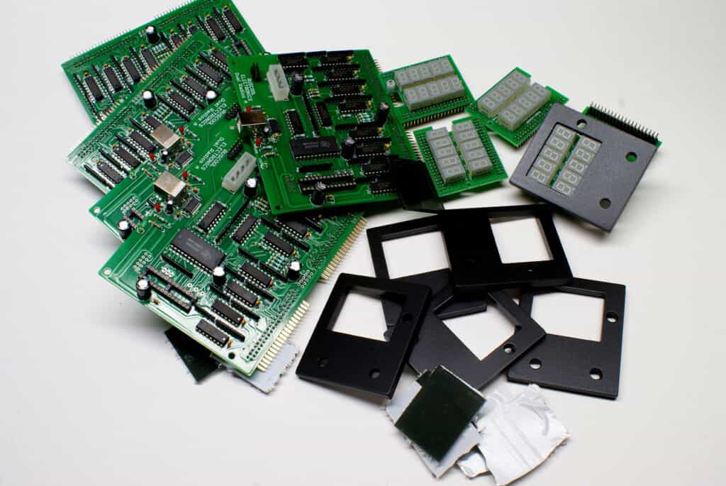
What are Printed Circuit Boards?
The printed circuit board helps in carrying electrical circuits. Also it permits the routing of power and signals between different devices. In addition, the printed circuit board is composed of some layers of material. These layers play an important role in PCB fabrication. Let’s go into details.
Substrate
Found at the board’s core is a base material, or substrate. The traditional boards make use of a fiberglass material referred to as FR4. However, other circuit boards might make use of ceramic, aluminum, and polymer substrates.
Copper
The substrate of a printed circuit board is usually covered with thin copper foil. Asides from the copper foil, it is laminated with adhesive and heat. The specific number of layers present in a circuit board has to do with the number of the copper layers. Also, majority of printed circuit boards have an ounce of copper foil for every square foot. Although the high-power printed circuit boards might use two or about three ounces.
The combination of these materials happens during the entire PCB fabrication process when creating the bare printed circuit board. Furthermore, the bare PCB passes the PCBA assembly in application of electronic components and solder, leading to a completely functional PCB. Copper foil
What is Printed Circuit Board Fabrication?
The PCB fabrication process deals with the combination of the board’s aforementioned materials in the functional layers in forming bare printed circuit boards. This is the process by which printed circuit board pcb fabrication works
Review of the Design
PCB fabrication process doesn’t begin till the engineering team has been able to review the design. This is referred to as Design for Manufacturability check. Also, this makes sure there is a valid design and it fulfills the specifications and tolerances could be met during the pcb SMT manufacturing process.
Application of the Film
This stage involves the printing of the PCB design onto the films making use of the laser direct imaging. This offers the photo negatives of your circuit board layout. Furthermore, the films are then applied onto the material layer, which then serves as a guide for every manufacturing process.
Copper Etching
Making use of different methods, the exposed copper or excess copper is removed or etched to help in creating pads and traces. This stage of PCB fabrication usually deals with multiple cleaning rounds. This is to get rid of the unwanted chemicals and excess material.
Lamination and Layer Stack-up
For the multilayer boards, the outer and inner layers are all aligned together after the process of copper etching. Usually this is achieved making use of the alignment holes present in the circuit board.
After the inspection of the layers, between every layer, there is an epoxy resin based prepreg placed between them. Also, this circuit board is then laminated together with the application of heat. The heat helps in melting the epoxy resin, which then adheres all the layers together.
Drilling
After laminating the circuit board layers together, you create holes into the circuit board using the drill. The holes created are useful for mounting the vias, through holes and holes.
Plating
After drilling, you plate the circuit board with a micron thick copper layer. Also, this coats the inner part of your drilled holes thereby creating the plated through-holes. Usually, this follows up with additional etching as well as copper removal on the board’s outer layer.
Application of the Solder Mask
After completing the copper layers, next in the PCB fabrication process is the cleaning of the panels and then covered with the solder mask. This solder mask is what gives the printed circuit boards its common green color
Furthermore, this solder mask helps in insulating the copper traces from the accidental contact with other conductive materials which can create some functional issues as well as help during the printed circuit board assembly process so that the solder will be applied to the right locations only.
Immediately it is applied, you remove the unwanted solder mask areas and the printed circuit board is then put in the oven to cure the layer of the solder mask.
Silkscreen
On the topmost area of your solder mask is the area where the application of the silkscreen layer takes place. Usually, this silkscreen is white in color and it add symbols, numbers, and letters to the PCB. Furthermore, the silkscreen layer assists with the location and types of the component during the PCB assembly.
Surface finishing
After curing the solder mask as well as the silkscreen, you can plate the printed circuit board with either silver or gold or other surface finishes. This ensures functionality and protection. This marks the end of the PCB fabrication process.
Why PCB Fabrication is Necessary?
The PCB fabrication is known as a specific outsourced activity whereby the third-party manufacturer makes use of the designs that customers provide. The impact of fabricated boards is seen in these areas.
Manufacturability
Choices with design affect PCB manufacturability. This is why PCB fabrication is important. The designs of the circuit board must consider the board’s material properties as well as permit adequate clearance in-between surface elements.
Yield rate
There are circumstances whereby you can fabricate these boards successfully making use of an existing design. Moreover, some design choices might cause PCB fabrication issues which causes many boards to be unusable
Reliability
Majority of boards are usually regulated under the specifications of the industry. This helps in dictating the necessary performance reliability level. When you fail to follow the industry requirements, it could cause nonfunctional or unreliable boards.
Conclusion
Printed circuit board (PCB) fabrication process involves working with the DFM (design for manufacturability) rules and checking the abilities and capabilities of the PCB manufacturer all through the PCB design cycle.
