When discussing dimensions that manufacturers utilize to produce printed circuit boards, it is crucial to also talk about standards that apply in this manufacturing process. Even though there isn’t any particular standard on the thickness that exists (officially), most manufacturers prefer to utilize certain thickness ranges on their PCBs. These preferred printed circuit board thickness ranges are highly recommended as they simplify the designing phase of your printed circuit board. Moreover, these thickness ranges leverage the PCB manufacturing gadgets, and they minimize the cost of production, helping you deliver a cost-effective, high-quality printed circuit board.
However, printed circuit board thicknesses can vary significantly due to client specifications and the board’s application. Due to these reasons, you might find yourself leaning more toward the thick printed circuit boards. These are copper-printed circuit boards that have a thickness range of 105 – 400 µm. But what advantages do you get from generating and using thick printed circuit boards? Is their performance better when compared with standard printed circuit boards?
Standard PCB Thickness
Generally, the standard printed circuit board thickness that most companies utilize is a PCB thickness of 1/16 inches. For most PCB manufacturing companies, this printed circuit board thickness range has become a standard. The reason behind this particular PCB thickness range is the fact that Bakelite sheets have a thickness of around 1/16 inches. And since manufacturers mainly relied on this material for PCB fabrication, this thickness became a standard. Now, most, if not all, PCB manufacturers generate PCB with this thickness as the standard thickness.
However, even though this is the most common PCB thickness, there are other printed circuit board thickness variations that exist. The other common standard thickness variations you can find when dealing with PCBs are 0.093-inch and 0.031-inch PCB thickness variations. These printed circuit board thickness variations are pretty popular because they meet the requirements of multilayered or robust PCBs.
Generally, PCBs might have other thicknesses outside and within this range. However, the thickness ranges above are the most common ones in the PCB industry.
Thick Copper Printed Circuit Boards
Printed circuit board can have a PCB copper thickness 0.5oz – 20oz. However, once you start approaching the 20oz territory, then you know that you are moving towards generating a thick PCB. PCB within and close to the 20 oz range are printed circuit boards that output and handle high currents hence their great thickness. Moreover, these PCBs have impeccable thermal management; therefore, they can handle high currents without burning out a task that would be impossible when using standard copper thicknesses.
Thick copper-printed circuit boards allow large circuit board-cross sections for impeccable current loads. Moreover, they also encourage impeccable heat dissipation, which is essential for their application areas.
When it comes to design, thick copper PCBs mostly come in two variations, double-sided or multilayered. Moreover, with this printed circuit board tech, it is possible to bring together a thick Cu (copper) layer on the inner board layers and fine layout PCB structures on the outer parts of the PCB.
Performance Qualities of a Thick Copper Printed Circuit Board.
Generally, thick copper-printed circuit boards have impeccable elongation performance. Moreover, due to their excellent heat dissipation, they are not limited by various features such as processing temperature, which makes them great for multiple applications. You can utilize these circuit boards on hot melt welding techniques, for example, oxygen blowing, which involves high temperatures. Moreover, these circuit boards do not become brittle when you expose them to lower temperatures.
When you utilize this thick circuit board in corrosive environments, the copper circuit board will generate a non-toxic shield layer to protect it from the environment. Therefore, as far as performance is concerned, thick PCBs are pretty efficient and reliable.
Advantages of Thick PCBs
Thick copper-printed circuit boards have multiple applications in multiple areas. For example, these circuit boards come in handy in the following application areas:
– High-tech gadgets
– Electronic equipment
– Medical gadgets
– Military gadgets
Moreover, thick copper-printed circuit boards on electronic gadgets give their core component (the circuit board) a more extended service life. Additionally, these circuit boards are pretty helpful in terms of size reduction when dealing with electronic equipment.
In printed circuit board prototypes, thick PCBs belong to the particular tech category that involves PCBs with operating difficulties and technical thresholds. Moreover, compared to other printed circuit boards, these PCBs tend to be relatively expensive.
Thick PCB Specifications

Though most printed circuit boards have the following copper thickness range:
– 0.1 mm thick PCB to 6.5 mm thick PCB
Standard PCBs tend to fall in the 1.57 mm or 0.62 inch thickness range. Anything below that leads you to thin PCBs, and anything beyond that leads you to thick printed circuit boards. However, since we are looking at thick printed circuit boards, here are some specifications of this particular PCB:
Materials
To generate high-quality thick copper printed circuit boards, most manufacturers will utilize the following components:
- FR4 –high Tg (170 degrees Celsius)
- FR-4 standard Tg (140 degrees Celsius)
When you combine these materials with the thickness of thick copper PCBs, you get a reliable and durable PCB that is able to handle harsh working conditions.
Track/Spacing
The minimum track/spacing for thick copper-printed circuit boards is as follows:
- For the external layer – when dealing with the external layer, the minimum spacing will be 60zo copper 12mil/15mil, 5 oz copper 12mil/15mil4 oz copper 10mil/13mil.
- For the internal layer – on the other hand, when you are dealing with internal layers, then the minimum spacing will be 6oz copper 12mil/12mil, 5oz copper 10mil/10mil, 4oz copper 8mil/8mil.
Minimum Hole Size
When dealing with thick printed circuit boards, you will be using the following minimum hole size:
- 1.15 mm – 0.3 mm
Maximum Outer and Inner Layer Cu Weight
The maximum outer layer Cu weight of a thick copper printed circuit board is usually:
- 13oz
On the other hand, the max inner layer Cu weight of a thick copper printed circuit board is the following:
- 12oz
Surface Finishes
When generating thick printed circuit boards, most manufacturers utilize the following surface finishes on the board:
- Enepig
- Immersion Silver
- Hard Gold
- OSP
- Immersion Gold
- HASL Lead-Free
- Solder Mask
On the other hand, to genera a unique thick copper PCB, most technicians utilize the following solder mask variations:
- Matte green
- Matte black
- Purple
- Black
- White
- Yellow
- Red
- And finally green
Via Process
Most, if not all, thick-printed circuit boards support the following via processes:
- Plugged vias
- Tenting via
- Uncovered vias
Factors Impacting Printed Circuit Board Thickness
While it is crucial to stick with the standard copper PCB thicknesses, multiple factors might lead to you choosing thick PCB variations. The most vital factors that impact the thickness of a PCB are design and production. Therefore, we shall divide the factors affecting printed circuit board thicknesses into two categories as follows:
Design Factors
Design factors are generally considered in the printed circuit board designing phase. However, these crucial factors tend to focus mainly on the purpose and functionality of the PCB instead of concentrating on practical consideration necessities that occur during production. The most vital design factors that impact printed circuit board thickness include the following:
Flexibility, Weight, and Size
Thinner printed circuit boards tend to be lighter when you compare them with thick PCB. However, thin circuit boards tend to bend and break more easily when compared to their denser counterparts. Therefore, if you want durability and reliability, you should consider catering for that extra cost to get a thick printed circuit board.
However, flexible printed circuit boards must be thin to effectively achieve the flexibility that makes them flexible PCBs. But if you are dealing with rigid printed circuit boards that don’t need flexing abilities, you will benefit significantly from thicker ones.
However, you should note that thick-printed circuit boards are more rugged. Moreover, these circuit boards are heavier and tend to occupy more space on your gadget. These two features tend to cause issues for people looking to generate lightweight devices or technicians looking to develop compact gadgets. Therefore, before you decide to create and use a thick printed circuit board, you have to know how you will use the board.
Copper Thickness
Generally, copper (Cu) thickness tends to play a significant role in the thickness of a printed circuit board. That is because the copper thickness tends to vary according to how much current passes through the circuit board. Generally, standard Cu thickness is 1.4mils – 2.8mils. However, you can adjust this thickness to meet the specifications of your printed circuit board. But it would help if you remembered that the thicker the Cu layer, the thicker your circuit board will be at the end of the production process. Moreover, the more copper you utilize on your circuit board, the more expensive the board will be since copper tends to be costly.
Board Materials
The lifetime and operation of a printed circuit board depends on the materials that you utilize to make it. If you use durable materials, your output will be a durable printed circuit board and vice versa. However, the materials that you utilize will also determine your board’s thickness. Typically, copper PCB fabrication involves the use of the following components:
- Silkscreen
- Solder mask
- Laminate
- Substrate
However, out of all these components, the most crucial ones are the substrate and the laminates. That is because these two components provide the board’s structure and impact the circuit board’s thickness significantly.
The circuit board substrate might consist of epoxy resin and paper, ceramic or glass weave, depending on your specified dielectric constant. On the other hand, laminates consist of a unique component known as thermoset resin which is combined with a cloth or a paper layer.
Generally, substrates and laminates come in multiple variations, and each variation affects the mechanical, electrical, and thermal properties of a circuit board in a unique way. Moreover, each variation impacts the overall thickness of a circuit board. Therefore, if you are going for a thick printed circuit board, this is a factor you should consider.
Printed Circuit Board Layers
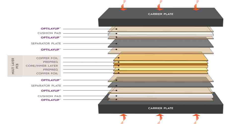
Typically, the number of circuit board layers you insert on your printed circuit board layout will undoubtedly impact your board’s thickness.
If you apply 2-6 layers on your printed circuit board, then it will most probably fall in the standard thickness threshold. However, using more than eight layers on your printed circuit board will take your PCB into the thick printed circuit board thickness threshold.
Manufacturing Factors Impacting Printed Circuit Board Thickness
Although design specifications impact the thickness of a circuit board more, manufacturing factors also play a vital role in the thickness level you select. Some major manufacturing factors that you should consider before choosing a thick PCB include the following:
Drill Hole Equipment
Even though most PCB designers focus on the drill hole spacing and size to achieve performance objectives, you should note that drill hole production processes tend to add complexity to the manufacturing process of PCBs. When drilling THT holes of any kind, fabricators are usually limited by the board’s thickness and the depth and diameter of the drilling lasers and machines. Therefore, thick printed circuit boards tend to give fabricators a hard time during the drilling phase of the printed circuit board, which ultimately drives the production cost of the PCB up.
Layer Count
As we saw earlier, the more PCB layers you utilize to make your circuit board, the thicker it will be at the end. However, while top-tier PCB manufacturers have the skills and gadgets to generate high-quality PCB bearing multiple layers, the capability isn’t universal. Moreover, the top-tier PCB manufacturing companies offering this service tend to do so at a high cost.
Conclusion
Thick-printed circuit boards are efficient PCBs that offer impeccable durability, reliability, and performance. And even though they cost relatively more when you compare them with standard PCBs, their efficiency compensates you. Therefore, if you want to purchase or produce a thick printed circuit board, try it out. However, it would help if you kept in mind all the factors we have gone through in this article to achieve a functional and practical thick-printed circuit board.
