3PDT switches are an essential component in guitar effect pedals. They are used to toggle between different effects or bypass the pedal entirely. The layout of the 3PDT switch on a printed circuit board (PCB) is crucial for the proper functioning of the pedal.
The 3PDT PCB layout is a critical aspect of designing a guitar effect pedal. The layout determines the placement of the switch and the connections between the switch and other components on the PCB. A well-designed layout ensures that the switch operates correctly and that the pedal functions as intended. In contrast, a poorly designed layout can lead to problems such as noise, signal loss, or even damage to the pedal.
Designers must consider several factors when creating a 3PDT PCB layout. These factors include the size and shape of the PCB, the placement of other components, and the routing of the wires. The layout must also be optimized for manufacturability, ensuring that the PCB can be produced efficiently and cost-effectively. By paying close attention to the 3PDT PCB layout, designers can create high-quality guitar effect pedals that meet the needs of musicians and sound engineers.
Basics of 3PDT PCB Layout
Why is 3PDT PCB Layout Important?
3PDT (3-pole double-throw) switches are commonly used in electronic circuits to switch between two different signal paths. They are widely used in guitar pedals, audio mixers, and other electronic devices. The proper layout of a 3PDT PCB is crucial for the overall performance and reliability of the circuit. A poorly designed layout can lead to signal distortion, noise, and other problems.
Key Considerations for 3PDT PCB Layout
When designing a 3PDT PCB layout, there are several key considerations to keep in mind:
- Signal Path: The signal path should be as short and direct as possible to minimize signal loss and interference.
- Grounding: Proper grounding is essential to minimize noise and interference. Ground traces should be kept as short as possible and connected directly to a common ground plane.
- Component Placement: Components should be placed in a logical and organized manner to minimize the length of signal paths and reduce the risk of interference.
- Trace Width: The width of traces should be carefully calculated to ensure that they can handle the required current without causing voltage drops or other issues.
Common Mistakes to Avoid in 3PDT PCB Layout
Here are some common mistakes to avoid when designing a 3PDT PCB layout:
- Crowded Layouts: Crowded layouts can lead to signal interference and make it difficult to troubleshoot and repair the circuit.
- Inadequate Grounding: Inadequate grounding can lead to noise and interference in the signal path.
- Poor Component Placement: Poor component placement can lead to longer signal paths and increase the risk of interference.
- Incorrect Trace Width: Incorrect trace width can cause voltage drops and other issues.
By taking these key considerations and common mistakes into account, you can design a 3PDT PCB layout that is optimized for performance and reliability.
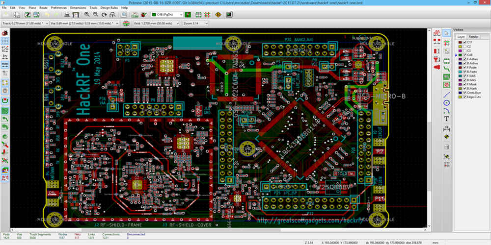
Designing a 3PDT PCB Layout

Tools and Software for 3PDT PCB Layout Design
Designing a 3PDT PCB layout can be a challenging task, but it can be made easier with the right tools and software. Here are some tools you’ll need to get started:
-
PCB design software: There are several PCB design software options available, such as Eagle, Altium, and KiCad. Choose one that suits your needs and budget.
-
3PDT footswitch: The 3PDT footswitch is the main component of the PCB layout. It allows you to switch between different circuits and effects.
-
Soldering iron: You’ll need a good soldering iron to assemble the PCB.
-
Multimeter: A multimeter is essential for testing and troubleshooting the PCB.
Step-by-Step Process for Designing a 3PDT PCB Layout
Here’s a step-by-step process for designing a 3PDT PCB layout:
-
Start by creating a schematic for your circuit. This will help you visualize the components and connections.
-
Once you have your schematic, create a new PCB layout in your chosen software.
-
Place the components on the PCB layout, keeping in mind the size and spacing requirements of each component.
-
Connect the components using traces on the PCB layout. Make sure to keep the traces as short as possible to minimize signal loss.
-
Add mounting holes and other necessary features to the PCB layout.
-
Check your PCB layout for errors and make any necessary adjustments.
-
Export your PCB layout files and send them to a manufacturer for fabrication.
Tips for Optimizing 3PDT PCB Layout Design
To optimize your 3PDT PCB layout design, consider the following tips:
-
Keep the traces as short as possible to minimize signal loss.
-
Use a ground plane to minimize noise and interference.
-
Use surface mount components to save space and reduce the size of the PCB.
-
Use a high-quality PCB manufacturer to ensure the best results.
By following these tips and using the right tools and software, you can create a high-quality 3PDT PCB layout that meets your needs.
Testing and Troubleshooting 3PDT PCB Layouts
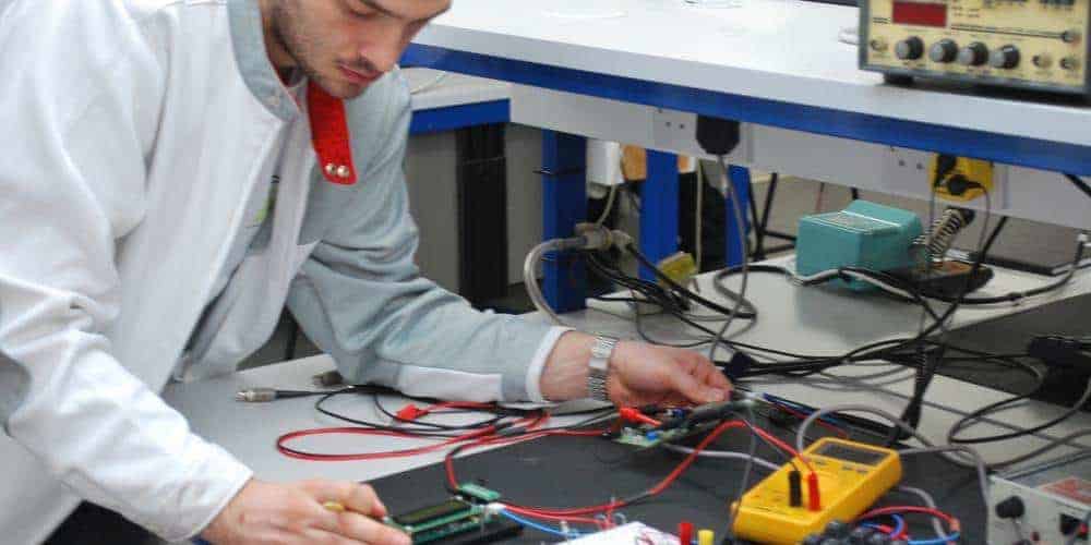
Testing a 3PDT PCB Layout
After assembling a 3PDT PCB layout, it is important to test it thoroughly to ensure that it is functioning as expected. The following steps can be taken to test a 3PDT PCB layout:
-
Check for continuity: Use a multimeter to check for continuity between the various components and traces on the board. This will help identify any open circuits or shorts.
-
Check for correct polarity: Verify that all polarized components such as diodes, capacitors, and transistors are installed with the correct polarity.
-
Test the switches: Use a multimeter to test the switches to ensure that they are functioning properly. Verify that they are making and breaking the connections as expected.
-
Test the LED indicators: Check that the LEDs are lighting up when the switches are activated.
Troubleshooting Common Issues in 3PDT PCB Layouts
Even after thorough testing, it is possible that issues may arise with the 3PDT PCB layout. Here are some common issues that may occur and their potential causes:
-
No sound output: This could be caused by a faulty connection between the input and output jacks, a short circuit, or a problem with the wiring.
-
Clicking or popping sounds: This could be caused by a faulty switch or a problem with the wiring.
-
Weak or distorted sound: This could be caused by a problem with the grounding or a faulty component such as a capacitor or resistor.
Best Practices for Debugging 3PDT PCB Layouts
When troubleshooting a 3PDT PCB layout, it is important to follow some best practices to ensure that the process is efficient and effective:
-
Start with the basics: Check that all components are installed correctly and that there are no obvious wiring errors.
-
Use a systematic approach: Start at one end of the circuit and work your way through it systematically, checking each component and connection along the way.
-
Use a multimeter: A multimeter can be an invaluable tool for identifying faults in a 3PDT PCB layout.
-
Be patient: Troubleshooting can be a time-consuming process, so it is important to be patient and methodical.
By following these steps and best practices, it is possible to effectively test and troubleshoot 3PDT PCB layouts.
