You will find PCB boards virtually everywhere in all gadgets used today. From your simple calculator to your Smartphone, their functions have to do with the performance of the printed circuit boards (PCBs). Now, do you have an idea of what composes PCB circuit boards or the bare boards? What makes these circuit boards so unique? What are the features that will make one circuit board more effective and productive than others?
If you want answers to all these questions, then stay calm. We’ve already prepared an informative guide that explains the materials useful for making PCBs. Let us begin by considering what the printed circuit boards are composed of. When concluding the article, we will explain ways that make sure you get the very best from an appropriate vendor.

What are PCB Circuit Boards or PCB Prototype Board Composed of?
Advanced circuits help in driving different electrical and electronic tools and equipment we use on a daily basis. Majority of PCBs are usually formed through the combination of at least two layers. Also, this depends on the nature and complexity of that particular device you’ll use them in.
Furthermore, printed circuit boards (PCBs) make use of different materials to get their composition. One of these layers could be manufactured from resin that is paper derived or fiberglass. You can use another base material like silkscreen layers, solder mask, and copper.
What are the Printed Circuit Board (PCB) Materials?
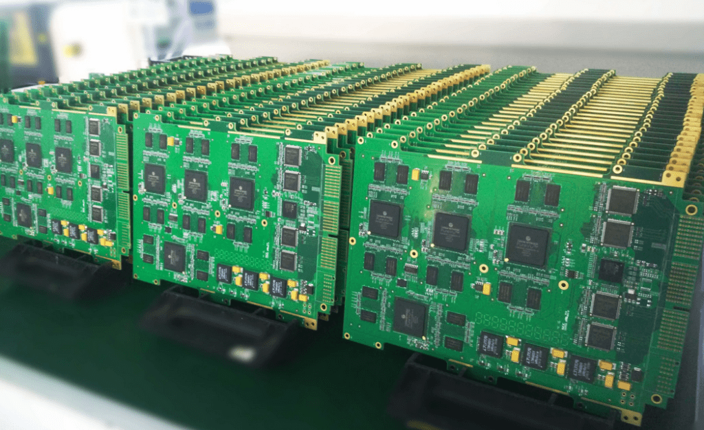
Generally, the printed circuit board is manufactured from four main layers, which are well bonded by pressure, heat, as well as other methods. These four layers include silkscreen, solder mask, copper, and substrate.
Those materials that are encompassed by printed circuit boards include:
Copper
Copper usually gathers on the foundation’s thick layer called the substrate. Depending on the type of board and use, there can be one or two copper layers present. The copper layer could exist on just one of the sides of the printed circuit board.
Also, it could be found on the two sides of the PCB substrate. Electronic devices, even the simple ones, use printed circuit boards that may have its copper layer just on one side. In contrast to the substrate, the copper layers are delicate and much thinner.
The copper plating utilized in the printed circuit board is usually referred to by the weight. Though the quantity of copper in the printed circuit board (PCB) helps in determining the quantity of power, it exchanges.
Silkscreen
Silkscreen makes the PCB (printed circuit board) to be readable to the technology programmers. They make this possible through the addition of letter and numerical indicators.
Substrate
Commonly, the substrate is referred to as FR4. This is also known as a fire retardant. It plays a role in offer a thick foundation layer for a printed circuit board. Sure, this varies; however, their thickness will change. This layer provides rigidity to the printed circuit board (PCB prototype).
You can also manufacture it from different flexible material that can be stretched as well. Of recent, there have been lots of innovative materials used for creating the substrate. At times, some are plant-based.
Soldermask
Note that other advanced circuits may not use these materials listed above. Rather, they use epoxies. One disadvantage that is applied to this commission type is their thermally sensitive nature. This makes them lose their lamination much quickly.
A very good way of recognizing the entire board type is via the smell they deliver anytime they are passing through the soldering processes using the soldering iron. The solder mask is the PCB top layer colored green, and it is usually applied all over that copper layer. This helps it come in contact with other electrical parts.
What are the Basics of Custom PCB Design?
To discuss the PCB design basis, you must be familiar with the background as well as the different terminologies. With reference to the schematic capture, we’ll go ahead to talk about a program permitting the operator to create the component’s schematic diagram, as well as other features.
This schematic capture represents this graphically. The different terminologies that are used here are:
PCB Layout Tool
This program involved in the PCB layout helps in permitting the structure of the wiring connection to apply it on many or multiple layers. Once completed, this operator will be able to create the needed CAD files to make your printed circuit board.
Gerber Files
The Gerber files or a gerber file deals with some design files that are computer-aided. These gerber files are sent to the printed circuit board (PCB) manufacturer to help in building the PCB layer structure.
What are the Steps in Custom PCB Design?
During our present age, available are some approaches that help in designing the PCB. There are so many ways of achieving this. This depends on the PCB manufacturer and PCB artist. Here are the important steps that you should take note of when designing the PCB.
Using a software
This has to do with designing PCBs making use of software. This has to do with the schematic representation of those advanced circuits using the software. The layout software you can use includes eagle software, mutism, and computer-aided design (CAD).
The Film Generation
When you make use of the completed circuit board diagram of the PCB layout, then you are making the film generation.
Choosing the raw materials
Simple devices usually make use of affordable PCBs that are produced from a paper phenolic with a copper foil bonding. The copper-clad laminate value is about 0.059 thick, with either the double-sided or single-sided board.
Drilling holes
The hole in PCBs is implemented making use of a machine as well as drill bit. The hand machine is the first machine type used for drilling holes in the PCB. Furthermore, the second machine is automatic in nature and called the CNC machines. The device needs the operator to put some efforts in making holes in the bare boards.
Fixing of the Image
The laser printers are great when printing the PCB layouts. The whole process includes
- Placing the clean copper layer on your printer
- Storing your design layout film on your computer
- Printing out the command that the computer receives from the laser printer
Etching & Stripping
The etching & stripping stage makes use of different chemicals to get rid of any unwanted copper that has attached itself onto the PCB.
Testing
Once you are through with the process above, the circuit board will undergo testing to be sure of its functionality. Recently, the manufacturing of many devices have taken place to help in testing the huge volumes of the PCBs.
What are the Custom PCB Design Rules?

There are rules linked with PCB design, which makes use of it effectively. There’s a need to take note and remember it.
Spacing and Width
For the spacing and width, these parameters are denoted as the x/y rules. Here, the X denotes the minimum trace width. The Y on the other hand, denotes the Spacing (minimum trace spacing).
Size and Thickness of the Board
The thickness and the size could help in suiting that particular product. So many individuals make use of more circuit boards on a panel to help in conserving cost and space and cost, when mass production has been completed.
Custom PCB Layout Design
The PCB layout design needs the professional skills and technical know-how which requires you to have a good knowledge of the PCB software, computer-aided design (CAD) system, as well as the methods or skills that are necessary to transfer the main circuit design successfully to the eventual PCB.
Furthermore, when comparing the PCB, there are some factors that you need to watch out for. These include
- The board size
- Available layers
- Differential pair routing
- 3D modeling
Important Steps in Custom PCB Layout
In this section, we will be explaining in detail the steps involved in custom PCB layout.
Converting the schematic into a PCB
This is the first ever step. Once you are through with the schematics, all you need to do is click “convert to PCB” on whatever editor you are using
Dragging and dropping the component
This next step has to do with the placement of the document where it should be positioned. If you prefer your PCB having a clean look, then you must place the components having a similar function side by side
Sketching the custom outline
Here, you’ll visit the layer menu and then select the board outline layer. After this, click the present outline and then delete it once you are done completing the new system using the PCB tools
The copper area
This area is thought of when there are many parts joined together to get a signal. Making use of the tools menu, you can create the copper area.
Routing
With respect to the current type, two approaches are available for this method. You can make use of an auto-router function if you are making use of low current in creating your PCB. Also, if having different track sizes is important, you can handle this manually. You can find this auto-router function on the topmost part of the page
Holes
There might be a need to mount the circuit boards on something. This is where the significance of holes comes in. You can find the hole tool in your tools menu, and then go ahead to locate that specific spot you desire
Text and Pictures
For this, you will have to stroll to your tools menu. Here, you will locate either the text or image tool. Also, you will be able to position the text the best way you like and then change the necessary layer. You can even change the book.
Photo view
Once you are done with all the steps outlined above, you can now round up the work by viewing your result. Also, you have the opportunity to alter the color, as well as other features. Immediately you are satisfied with your product, select “fabrication output” to purchase the PCB.
Custom Made Printed Circuit Boards
Already, we know that PCBs are very complex elements. This is why it could be a little difficult for the hobbyists to design a working circuit all by themselves. The very first important thing is having reliable software ready for creating your PCB’s blueprint.
After this, you can utilize many solutions like Eagle that does a great gob in PCB design.
Preparation of the Schematic View
Preparation of the schematic view is necessary to be able to create the custom PCB.
Visit the component library, which is in the design software and then place them on the canvas. Now, you will need to connect your pins with those lines symbolizing the software’s electrical connections.
This same part number could confuse you a little because there will be different options for you to select from. Also, these different packages could include dual-in-line box and surface-mounted chip.
Furthermore, if you’re working on a DIY project, then choosing a noticeable and significant DIPs or system-in-packages is the best option. Finding them can be done quickly, while the hobby outlets are usually much more friendly when you are selling them in contrast to the surface-mounted devices that are specially reserved for the commercial applications.
Also, the packaging options could look similar in that schematic view. However, some things will begin to look different whenever you decide to switch to the layout view to start the design.
More on the schematic view

Furthermore, there’ll be a need to offer the required power and ground signals asides from the placement of your components and interconnections. In addition, you can make use of the features like VCC, VDD, and GND seen in the library of Eagle
Also, always remember to integrate the board’s connectors to ensure that you can employ the power and the ground. During this stage, you’ll have your desired external device like LEDs or potentiometer.
After this, the design has to pass through the ERC (electrical rule check) once everything has been put in place. The significance of this test cannot be overemphasized because it ensures no errors in your advanced circuits. If there are errors, this will affect the circuit board’s functionality.
Some issues you may likely face include wires appearing connected, however they aren’t real Using the Eagle software, it is possible to check the little dots that represents the wires’ connection intersections
Other possible issues include power and ground signals which you didn’t remember to connect.
Layout View of the Access Board
After completing the necessary things for the schematic view, the next step is activating the circuit board layout view. Now, you have already made the switch and the components will be spread about randomly in the Eagle software. Also, you will see that the wires are directly hooking to the pins
To ensure that the picture is less messy, continue moving these components until they start to make meaning. For instance, you may move these components to the edges to ensure that things start making sense
There is still much to do before having your circuit board. Therefore, there is a need to dedicate these signals to all the layers. However, keep it in mind that the layers in one layer must tough themselves
Eagle’s professional version has the auto-layout feature. This helps in routing the signals with just one click. Moreover, for those using the standard version, they have to find a solution themselves. Also, you can work with a PCB manufacturer to find the design solution and handle this step.
After laying down these signals, then you are ready to run the design check or DRC. This check makes sure that the drilling of the holes is done near a signal line. Also, this check will notify you when the traces are at the board’s edge or aren’t at a specific optimum.
More on the Layout view
Also, it is possible to customize the rules. At times, the PCB vendor offers a specific file which you can integrate with the Eagle solution with the specific DRC values. Next, you can continue and then upload the design files immediately the project passes the design check.
Furthermore, you should make use of a specific layer in adding the silkscreen lettering onto the top. This printing assists you in knowing which of the components fits. With this, you can avoid errors and mistakes.
In addition, the gerber file tells the PCB design language. Also, each board will be able to have a lot of files linked with them. There will be a different file for the solder pads specifications and different files for every layer. These drill files will also carry the drilling specifications.
Then, you may upload the design with the manufacturer. The manufacturer will make use of a different program in presenting the last look of these layers. Also, you will discover if these components have the perfect size for the holes.
By this, we have concluded on how to create the custom PCB making use of the design software.
Conclusion
Here comes the end of our article on custom PCB. We hope you have taken time to read and understand every detail.
