EDA design, or electronic design automation, is a crucial part of the modern electronics industry. It involves the use of software tools to design and analyze electronic systems, from individual components to entire circuits. EDA design has become increasingly important as electronic devices have become more complex and sophisticated, and as the demand for faster, more powerful, and more energy-efficient electronics has grown.
One of the key benefits of EDA design is that it allows engineers to simulate and test electronic systems before they are physically built. This can save time and money, as well as reduce the risk of errors and design flaws. EDA design tools can also help engineers optimize their designs for factors such as power consumption, signal integrity, and thermal performance. In addition, EDA design enables engineers to collaborate on complex projects more easily, as they can share designs and data electronically.

What is EDA Design?
EDA, or Electronic Design Automation, is a category of software tools used for designing electronic systems such as integrated circuits (ICs) and printed circuit boards (PCBs). These tools are used by electrical engineers and designers to automate the design and verification of complex electronic systems.
EDA design tools are essential for designing electronic systems as they allow engineers to perform complex tasks such as schematic capture, simulation, and layout design. These tools also enable designers to optimize their designs for performance, power, and cost.
EDA design tools have evolved over the years, from simple schematic capture tools to complex software suites that include simulation, verification, and layout design capabilities. Today, EDA design tools are used by engineers and designers to design everything from simple digital circuits to complex mixed-signal systems.
In summary, EDA design is the process of designing electronic systems using software tools that automate the design and verification process. These tools are essential for designing complex electronic systems and have become an integral part of the electronics industry.
The Importance of EDA Design
EDA (Electronic Design Automation) is a crucial process in the development of electronic systems, circuits, and devices. It is a set of software tools that helps in designing, analyzing, and simulating electronic circuits. EDA design plays a vital role in the success of any electronic product development project. Here are some reasons why EDA design is important:
1. Reduces Time-to-Market
EDA design tools help in reducing the time-to-market of electronic products. The design process is automated, and hence, it takes less time to complete the design phase. EDA tools also help in identifying design errors and issues before the manufacturing stage, which saves time and reduces the risk of costly mistakes.
2. Improves Design Quality
EDA design tools help in improving the quality of electronic designs. They provide a wide range of design analysis and simulation capabilities that help in identifying design flaws and errors. EDA tools also help in optimizing the design for performance, power consumption, and cost.
3. Enhances Productivity
EDA design tools help in enhancing the productivity of the design team. They automate repetitive tasks and provide a user-friendly interface that simplifies the design process. EDA tools also help in collaboration between team members by providing a centralized design database.
4. Reduces Development Costs
EDA design tools help in reducing the development costs of electronic products. They provide a cost-effective way to design and simulate electronic circuits. EDA tools also help in identifying design errors and issues early in the design process, which reduces the cost of rework and redesign.
In conclusion, EDA design plays a critical role in the success of electronic product development projects. It reduces time-to-market, improves design quality, enhances productivity, and reduces development costs. EDA design tools provide a cost-effective and efficient way to design, analyze, and simulate electronic circuits.
EDA Design Process

The EDA (Electronic Design Automation) design process is a systematic approach to designing and verifying electronic circuits. The process involves several stages, each with its own set of tools and techniques.
Design Specification
The first stage of the EDA design process is the design specification. This stage involves defining the requirements and specifications of the circuit to be designed. The designer must identify the functionality, performance, and other requirements of the circuit. This stage is critical as it forms the basis of the entire design process.
Design Entry
Once the design specification is complete, the designer moves on to the design entry stage. In this stage, the designer creates a schematic or a block diagram of the circuit. The schematic represents the circuit’s components and their interconnections. The designer can use EDA tools to create the schematic, which can then be verified for correctness.
Simulation and Analysis
After the schematic is created, the designer moves on to the simulation and analysis stage. In this stage, the designer simulates the circuit’s behavior using EDA tools. The simulation helps the designer identify and correct any errors or issues in the design. The designer can also analyze the circuit’s performance using various analysis tools.
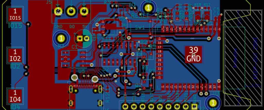
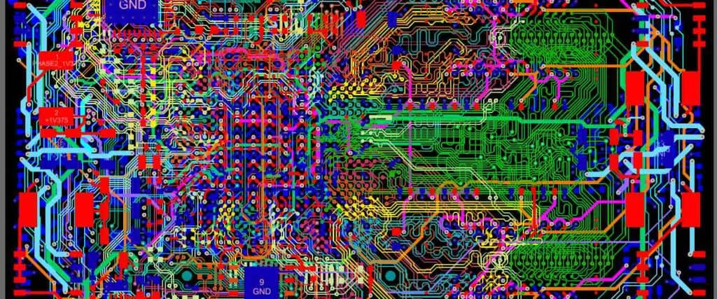
Layout and Routing
Once the circuit’s behavior is verified, the designer moves on to the layout and routing stage. In this stage, the designer creates a physical layout of the circuit. The layout represents the physical placement of the components on the circuit board. The designer can use EDA tools to optimize the layout and routing to minimize noise and interference.
Verification and Testing
The final stage of the EDA design process is the verification and testing stage. In this stage, the designer verifies the circuit’s functionality and performance. The designer can use various testing tools and techniques to ensure the circuit meets the design specification.
Overall, the EDA design process is a systematic approach to designing and verifying electronic circuits. The process involves several stages, each with its own set of tools and techniques. By following the EDA design process, designers can create high-quality, reliable, and efficient electronic circuits.
EDA Design Tools
EDA (Electronic Design Automation) tools are software programs used by engineers to design, analyze, and simulate electronic circuits. These tools are essential for creating complex circuit designs and ensuring that they function correctly.
There are several EDA design tools available in the market, and each tool has its unique features and capabilities. Some of the most popular EDA design tools are:
-
Altium Designer: Altium Designer is a powerful and easy-to-use EDA tool that provides a unified design environment for creating complex electronic circuits. It offers a wide range of features, including schematic capture, PCB layout, and 3D visualization.
-
Cadence Allegro: Cadence Allegro is a comprehensive EDA tool that provides a complete solution for designing and analyzing electronic circuits. It offers a range of features, including schematic capture, PCB layout, and signal integrity analysis.
-
Mentor Graphics PADS: Mentor Graphics PADS is a user-friendly EDA tool that provides a complete solution for designing and analyzing electronic circuits. It offers a range of features, including schematic capture, PCB layout, and signal integrity analysis.
-
OrCAD: OrCAD is a popular EDA tool that provides a complete solution for designing and analyzing electronic circuits. It offers a range of features, including schematic capture, PCB layout, and signal integrity analysis.
EDA design tools are essential for creating complex electronic circuits and ensuring that they function correctly. These tools provide engineers with the necessary tools and features to design, analyze, and simulate electronic circuits. With the right EDA design tool, engineers can create high-quality electronic circuits that meet the required specifications and standards.
EDA Design Challenges
EDA design, or electronic design automation, involves the use of software tools to design and analyze electronic systems. While EDA tools have significantly improved the design process, they also present a number of challenges. Here are some of the most common EDA design challenges:
1. Increasing Design Complexity
As technology advances, electronic systems are becoming more complex. This means that designers must deal with more components, more interactions between components, and more potential sources of error. EDA tools can help manage this complexity, but they also require more powerful hardware and software to operate effectively.
2. Time-to-Market Pressure
In today’s fast-paced business environment, time-to-market is critical. Companies must get their products to market quickly to stay competitive. However, designing and testing complex electronic systems takes time. EDA tools can help speed up the design process, but they also require a significant investment in time and resources to learn and use effectively.
3. Design Verification
Design verification is a critical step in the EDA design process. It involves testing the design to ensure that it meets the desired specifications and is free from errors. However, as designs become more complex, the verification process becomes more difficult and time-consuming. EDA tools can help automate some aspects of the verification process, but they also require significant computational resources.
4. Cost
EDA tools can be expensive, especially for small design teams or individual designers. In addition, the hardware required to run EDA tools can also be costly. This can make it difficult for smaller companies or independent designers to compete with larger companies that have more resources.
5. Integration with Other Tools
EDA tools must often be integrated with other software tools, such as simulation tools or programming environments. This can be challenging, especially if the tools are from different vendors or use different file formats. EDA tool vendors are working to address this challenge by providing more open and flexible tools that can work with a variety of other software tools.
Overall, EDA design presents a number of challenges, but with the right tools and expertise, these challenges can be overcome.
EDA Design Trends
The world of EDA design is constantly evolving, and keeping up with the latest trends is essential for staying ahead of the competition. Here are some of the top trends in EDA design that are shaping the industry today.
Cloud-Based EDA Design
Cloud-based EDA design is becoming increasingly popular as more and more companies move their design processes to the cloud. This trend is driven by the need for more flexible and scalable design environments that can be accessed from anywhere in the world. Cloud-based EDA design also allows for more efficient collaboration between team members, as well as faster and more accurate design iterations.
AI and Machine Learning
AI and machine learning are revolutionizing the EDA design process by enabling designers to automate many of the tedious and time-consuming tasks involved in the design process. This trend is driven by the need to speed up the design process and reduce errors, as well as the increasing availability of powerful AI and machine learning tools.
Increased Focus on Security
With the growing threat of cyber attacks, security is becoming an increasingly important consideration in EDA design. This trend is driven by the need to protect sensitive design data and intellectual property from unauthorized access and theft. To address this challenge, companies are investing in advanced security technologies and best practices to ensure that their design processes are as secure as possible.
Emphasis on Power Efficiency
As electronic devices become increasingly complex and power-hungry, power efficiency is becoming an increasingly important consideration in EDA design. This trend is driven by the need to extend battery life and reduce energy consumption in electronic devices. To address this challenge, designers are focusing on developing more power-efficient designs that can operate for longer periods of time without needing to be recharged.
In conclusion, these are just a few of the top trends in EDA design that are shaping the industry today. By staying up-to-date with the latest trends and technologies, designers can stay ahead of the competition and deliver innovative, high-quality designs that meet the needs of their customers.
