Electrical engineering PCB design is an essential process in the development of electronic devices. PCBs, or printed circuit boards, serve as the backbone of electronic devices, providing a platform for the various components to be connected and communicate with each other. The design of a PCB can significantly impact the performance, reliability, and cost of an electronic device.
To design an effective PCB, electrical engineers must consider a range of factors, including the size and shape of the board, the placement of components, and the routing of electrical signals. They must also ensure that the board can withstand the environmental conditions it will be exposed to and that it meets any regulatory requirements. With the increasing complexity of electronic devices and the demand for smaller, more powerful devices, the importance of PCB design has only grown in recent years.
Basics of PCB Design
What is PCB Design?
Printed Circuit Board (PCB) design is the process of creating a layout for electronic circuits on a board. It involves designing the placement of components, traces, and vias, and the routing of electrical connections between them.
Why is PCB Design Important?
PCB design is a critical step in the development of electronic products. A well-designed PCB ensures that the electronic circuit functions correctly, is reliable, and meets performance requirements. Poor PCB design can result in electrical noise, signal interference, and even complete circuit failure.
PCB Design Process
The PCB design process involves several steps, including schematic capture, board layout, and manufacturing.
Schematic Capture
Schematic capture is the process of creating a graphical representation of the electronic circuit using specialized software. This representation shows the components and their connections.
Board Layout
Board layout involves placing the components on the board and routing the electrical connections between them. The layout must be optimized to minimize signal interference, noise, and other issues that can affect circuit performance.
Manufacturing
Once the board layout is complete, the design is sent to a manufacturer for production. The manufacturer creates the physical board, including drilling holes, applying a copper layer, and adding a solder mask.
In conclusion, PCB design is a crucial step in the development of electronic products. A well-designed PCB ensures that the electronic circuit functions correctly, is reliable, and meets performance requirements. The PCB design process involves several steps, including schematic capture, board layout, and manufacturing.
Electrical Engineering Principles for PCB Design

Circuit Design
Circuit design is the foundation of PCB design. It involves the creation of a schematic diagram that represents the electrical connections between components. The schematic diagram should be clear, concise, and easy to read. It should also be properly annotated with component values, reference designators, and other important information.
Signal Integrity
Signal integrity is crucial to the proper functioning of a PCB. It refers to the ability of a signal to maintain its quality as it travels through a circuit. To ensure good signal integrity, it is important to minimize noise and interference in the circuit. This can be achieved by using proper grounding techniques, minimizing the length of signal traces, and using high-quality components.
Power Integrity
Power integrity is the ability of a circuit to maintain a stable power supply. It is important to ensure that the power supply is clean and free from noise and interference. This can be achieved by using proper decoupling techniques, such as placing capacitors near power pins, and using separate power and ground planes.
Thermal Management
Thermal management is critical to the longevity and reliability of a PCB. It is important to ensure that the temperature of the PCB does not exceed the maximum operating temperature of the components. This can be achieved by using proper heat sinking techniques, such as placing heat sinks on components that generate a lot of heat, and ensuring proper airflow through the PCB.
In conclusion, good electrical engineering principles are essential to the design of a successful PCB. By following these principles, designers can create circuits that are reliable, efficient, and functional.
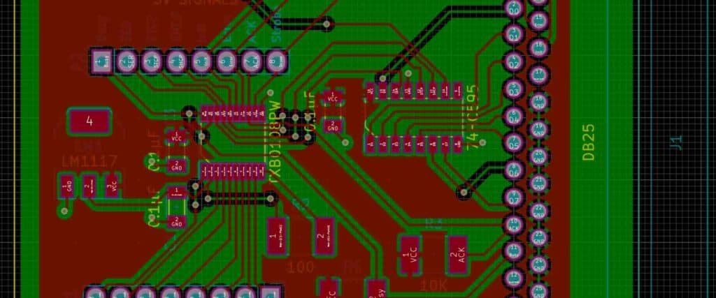
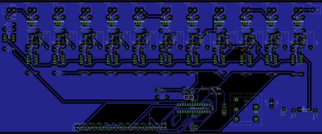
PCB Layout Design
PCB layout design is an essential part of electrical engineering. It involves designing the physical layout of a printed circuit board (PCB) to ensure that it meets the electrical and mechanical requirements of the circuit. A well-designed PCB layout can reduce the risk of errors and improve the overall performance of the circuit.
Component Placement
Component placement is a crucial step in PCB layout design. It involves deciding where to place each component on the board to optimize the circuit’s performance. Factors such as signal integrity, thermal management, and ease of assembly must be considered when placing the components.
Routing
Routing refers to the process of connecting the components on the PCB with traces. The routing process must be carefully planned to ensure that all the connections are made correctly and efficiently. The routing process must also consider the signal integrity and ensure that the traces have the correct impedance to avoid signal degradation.
Grounding and Power Planes
Grounding and power planes are essential components of a well-designed PCB. Grounding is necessary to ensure that the circuit has a stable reference point, and power planes are necessary to provide a stable power supply to the circuit. Proper grounding and power plane design can reduce noise, improve signal integrity, and reduce the risk of EMI.
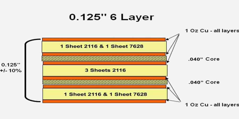
Stackup Design
Stackup design refers to the arrangement of layers in a PCB. The number of layers and the arrangement of the layers can have a significant impact on the performance of the circuit. A well-designed stackup can improve signal integrity, reduce noise, and improve thermal management.
In summary, PCB layout design is a critical aspect of electrical engineering. Component placement, routing, grounding and power planes, and stackup design are essential components of a well-designed PCB. By carefully considering each of these factors, engineers can design PCBs that meet the electrical and mechanical requirements of the circuit.
Design for Manufacturing
Design Rules and Constraints
When designing a printed circuit board (PCB), it is important to consider the manufacturing process from the beginning. Design rules and constraints are guidelines that ensure the PCB can be manufactured without errors or problems. These rules include minimum trace widths and clearances, minimum drill sizes, and minimum annular ring sizes.
Design constraints are specific requirements for the PCB design that must be met in order to ensure proper functionality. These constraints may include specific layer thicknesses, controlled impedance, or specific materials. By following these rules and constraints, the PCB can be manufactured with minimal errors and can function as intended.
DFM Checks
Design for Manufacturing (DFM) checks are automated tests that ensure the PCB design meets the manufacturing requirements. These checks include Design Rule Checks (DRC) and Electrical Rule Checks (ERC). DRC checks ensure that the design meets the minimum trace widths, clearances, and other design rules. ERC checks ensure that the design meets electrical requirements such as proper net connections, voltage, and current limits.
DFM checks can be performed using specialized software tools that analyze the PCB design and provide feedback on any errors or issues. By performing DFM checks, designers can ensure that the PCB design is optimized for manufacturing and will function properly.
Panelization
Panelization is the process of arranging multiple PCB designs onto a single panel for manufacturing. This process can help reduce manufacturing costs and improve efficiency. Panelization requires careful consideration of the PCB design, including the location of fiducial markers, routing between boards, and the placement of tooling holes.
Manufacturers may have specific requirements for panelization, including panel size, spacing between boards, and the number of boards per panel. By considering panelization during the design process, designers can ensure that the PCB design is optimized for manufacturing and can be easily integrated into the manufacturing process.
In conclusion, designing a PCB for manufacturing requires careful consideration of design rules and constraints, DFM checks, and panelization. By following these guidelines, designers can ensure that the PCB design is optimized for manufacturing and will function properly.
PCB Design Tools
When it comes to designing printed circuit boards (PCBs), there are a variety of software tools available to electrical engineers. These tools can help simplify the design process and ensure that the final product meets all necessary specifications and requirements.
Schematic Capture
Schematic capture software allows engineers to create and modify electronic schematics for their PCB designs. This software typically includes a library of electronic symbols and components, making it easy to quickly assemble a schematic. Some popular schematic capture tools include Altium Designer, Eagle PCB, and KiCAD.
PCB Layout Software
Once a schematic has been created, engineers can use PCB layout software to design the physical layout of the board. This software allows users to place components, route traces, and define board dimensions and layers. Some popular PCB layout tools include Altium Designer, Eagle PCB, and KiCAD.
Simulation Tools
Simulation tools can be used to test and verify the functionality of a PCB design before it is physically manufactured. These tools can simulate the behavior of electronic components and circuits, allowing engineers to identify and correct potential issues early in the design process. Some popular simulation tools include LTspice, PSpice, and Simulink.
Design for Testability
Design for testability (DFT) is an important consideration when designing a PCB. DFT tools can help engineers ensure that their designs can be effectively tested and diagnosed for any potential issues. This can include tools for boundary scan testing, in-circuit testing, and functional testing. Some popular DFT tools include JTAG Technologies and Teradyne.
Overall, the use of PCB design tools can greatly simplify the design process and help ensure that the final product meets all necessary requirements. By using a combination of schematic capture, PCB layout software, simulation tools, and DFT tools, engineers can create high-quality, reliable PCB designs.
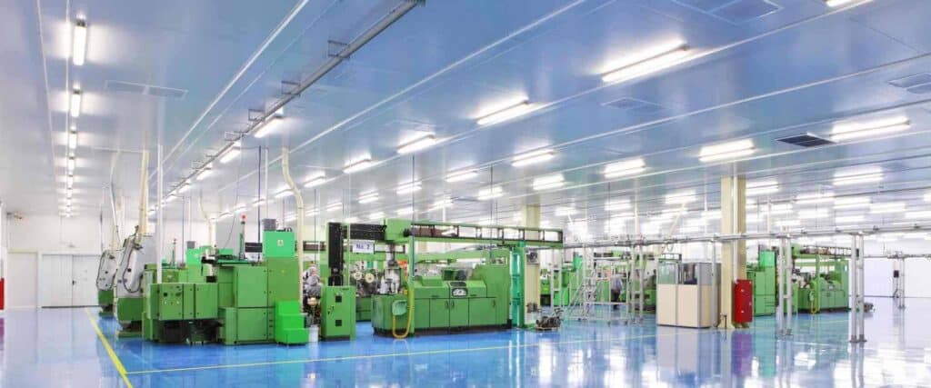
PCB Fabrication and Assembly
PCB Manufacturing Process
PCB fabrication is the process of creating a printed circuit board (PCB) from a substrate material. The process starts with a design file that is used to create a photomask. The photomask is then used to transfer the design onto a copper-clad board. The board is then etched to remove the copper not covered by the mask. The remaining copper forms the traces and pads of the circuit.
The PCB manufacturing process involves several steps, including drilling, plating, and solder masking. The drilling process creates holes for components and vias, which connect the different layers of the board. Plating adds a layer of copper to the drilled holes, making them conductive. Solder masking is the process of applying a protective layer to the board to prevent solder from flowing where it is not intended.
PCB Assembly Process
PCB assembly is the process of attaching electronic components to the PCB. The process involves several steps, including component placement, soldering, and inspection. Component placement involves using automated equipment to place components on the board. Soldering is the process of attaching the components to the board using molten solder. Inspection involves checking the board for defects and ensuring that all components are properly attached.
PCB assembly can be done manually or with automated equipment. Manual assembly is time-consuming and prone to errors, while automated assembly is faster and more precise.
Testing and Inspection
Testing and inspection are critical steps in the PCB fabrication and assembly process. Testing involves checking the board for electrical continuity and verifying that all components are functioning properly. Inspection involves checking the board for defects, such as solder bridges, missing components, and incorrect placement.
Testing and inspection can be done manually or with automated equipment. Automated testing and inspection are faster and more accurate than manual methods.
In conclusion, the PCB fabrication and assembly process is complex and involves several steps. PCB manufacturers and assemblers use automated equipment to improve efficiency and reduce errors. Testing and inspection are critical to ensure that the final product is of high quality and functions properly.
Conclusion
In conclusion, PCB design is a crucial aspect of electrical engineering. It is a complex process that requires careful planning and attention to detail. The design must be optimized to ensure that the circuit operates efficiently and reliably.
Throughout this article, we have covered the fundamentals of PCB design, including the various types of PCBs, the design process, and the tools and software used for designing PCBs. We have also explored the importance of PCB layout, including the placement of components and the routing of traces.
One of the most critical aspects of PCB design is ensuring that the design meets all necessary specifications and requirements. This involves considering factors such as signal integrity, thermal management, and power consumption.
To ensure that the PCB design meets all necessary requirements, it is essential to work closely with the manufacturer and to perform thorough testing and verification of the design before production.
Overall, PCB design is a complex and challenging process that requires a high level of skill and expertise. However, by following the guidelines and best practices outlined in this article, you can design PCBs that are efficient, reliable, and meet all necessary requirements.
