We will assume that you have an idea of the parts or components required for making your circuit board. So, we will get right into it. In this article, we talk about the FPGA PCB Design, how you should go about making the design and some of the differences between an FPGA and a PCB.
What is an FPGA Board?
Let us start by understanding the concept or FPGA basics. It stands for Field Programmable Gate Array. This means that the board can be reprogrammed, modified or reworked to fit into different uses.
Thus, the FPGA board meaning is that of an Integrated Circuit (IC), which can be configured or subjected to further optimization, after the initial production.
What is an FPGA PCB?
This is the fusion of two terms – FPGA and PCB. The latter refers to the Printed Circuit Board (PCB), a dedicated platform upon which many components can be placed or mounted to enhance the performance or workings of the consumer electronics.
The fusion leads to the integration of the FPGA into the existing PCB architecture to help improve the performance of the targeted devices.
Potential Bottlenecks to Making a Design with FPGA
As much as you can attach the component (FPGA) into the base card or main board (PCB) for assembly, certain bottlenecks tend to come up.
Understanding how these issues can influence the FPGA design is one major step to getting your way around them.
Here are some of the reasons why making this integration wouldn’t be smooth:
Floor-planning Issues
This is the major issue you will face with our FPGA design. Floor-planning has to do with the optimization of the board to enable the fitting or matching of the overall design concept.
Floor-planning becomes an issue also when you have figured out where the components or parts are to be placed on the board. Thus, integrating the FPGA in such an instance is a pathway to making design errors.
Another angle to how floor-planning influences the design is the matching of the board’s construction to the implementation of the configuration on the Field Programmable Gate Array (FPGA).
The Routing Path
You are not just thinking about the connection of the boards. You are also seeking out ways to facilitate the routing of the signals in the boards.
To this end, the stackup and routing channels in the FPGA should be considered as well.
What You Must Know About the FPGA PCB Specifications
When the chip connecting and supporting several components (PCB) is used with the electronic component (FPGA), you can say that what you have is the FPGA PCB.
Now, before getting around the design, you must take into account the important FPGA specifications. Usually, these are limited to the drill size and the trace/space. These specifics are usually measured based on a specified minimum or range.
For the drill size, it is expected that the minimum should be 0.2 millimeter. For the minimum trace/space, the consideration is usually on the minimum width of the trace and the minimal space between the copper features.
However, you must note that there are some additional key points that potentially contribute to the board’s specifications. These include:
- Interface Table: the work of the interface table is to help maintain an error-free FPGA PCB design, while keeping an excellent control of the interface.
- Current Margin: it is expedient to mention that the power rating of an FPGA PCB potentially influences the performance. If the power supply is low, you can be sure that the board wouldn’t live up to the full potentials. Therefore, maintaining a minimum current margin is a sure way to keep the board operating optimally.
How to Design FPGA Board as a BGA: What You Need to Know

Do you know that most of the Field Programmable Gate Arrays (FPGAs) are made into the Ball Grid Array (BGA) packages?
This is one of the reasons why you may have some challenges designing the board. These challenges cut across layout and routing of the board, due to the higher numbers of Inputs and Outputs (I/Os) used with the components.
Other issues that could come up include:
- Marginal Issues: these have to do with the challenges that allow for a part-working of the board. In this case, the FPGA could work in some instances and not work in other instances.
- Functional Issues: these refer to the inability of the FPGA PCB to operate as ought to. An instance could be the inability of the FPGA’s clock from functioning, due to the use of a different kind of clock pin.
- Electrical Issues: these are third kind of FPGA PCB design issues. They have to do with the problems arising from inappropriate or malfunctioning electrical connections on the board.
The FPGA PCB Design Guidelines
The best way to ensure the optimal performance of the Field Programmable Gate Array (FPGA)’s performance in the PCB is to follow the rules to the latter.
Here are some of the major FPGA PCB design guidelines to follow:
1. Implement the Proper BGA Stackups and Routings
Note that most of the FPGAs come in the form of Ball Grid Arrays (BGAs). Although you can also find variants like the QFPs, it is common to find more of the BGA-packages. As such, your board must be designed accordingly to enable the fitting into the BGA packages.
Following the right stackup design and routing method can help you achieve this. Here are some tips on how to go about it:
- The ground fill and ground planes should be used to support the use of impedance control to enable high-speed routing.
- The signal layers and power should be interleaved with the ground layers in the PCB’s stackup.
- If you are using the high-speed Inputs and Outputs (I/Os), it is important to ensure that the outer layer is thin. This helps to prevent the need for “necking-down” the outer layer.
- Another requirement for the FPGA PCB’s stackup is to use the standard BGA methods to determine the number of signals needed for routing the board.
2. FPGA PCB Footprint Verification
One important step in FPGA programming is the verification of the board’s footprint, as well as the fanout.
Start by checking if the NSMD vs. SMD pads are needed. The next step is to figure out if the via-in-pad is needed, especially as it is based on the ball pitch. The next verification process is determining the best ball clearance for traces in the routing channels. Once these three have been done, you can determine the appropriate layer thickness for impedance-controlled channels. This can be done by using the previous point.
3. Determine the Right Placements
Where the Field Programmable Gate Array (FPGA) is placed on the PCB is very important. The first process is by placing the FPGA in the form of a component. In this case, it is distanced from the PCB’s edges, as this enables a smooth extension of the routing channels.
A better way, however, is to use the System-on-Module (SOM) option. If you are following this method, the SOM must be the recommended one from either the component’s vendor or a verified third-party company.
Another point in the FPGA selection guide for System-on-Modules (SOMs) is that the board-to-board connectors must be “fanned out” to pave way for the SOM’s placement. Note that the connectors to be fanned out are mostly the ones having higher I/Os.
4. Select the Right Vendor IP for Silicon Implementation
With the placement options settled, you don’t have to jump right into routing the stackup. Instead, the next step would be the selection of the right vendor IP for the silicon’s implementation. The point is that if you choose the wrong IP, you might only spend more time working on the stackup – and it still wouldn’t come out as expected.
To this end, we suggest using only the recommended IP from your component’s vendor. Also, the IP should be used for the appropriate cases. The core uses are for implementing application-specific processing and standard digital interfaces that are not pre-packaged into the component.
Here are a few tips on the selection and implementation of the vendor IP:
- The implementation could start with the impedance requirements. This gives you ample time to figure out the PCB’s stackup, as the IP is normally used with the high-speed digital interfaces.
- You can use the vendor IP to expand or extend the available digital interfaces on the FPGA to a larger number. It is also possible to use the same to expand the aforementioned interfaces to a less popular interface, which might not be on the standard FPGA die.
5. Prepare the Routing Channels
This should be the last thing to do, as per the FPGA PCB design guidelines. The planning of the routing channels comes after you have satisfied that the FPGA’s footprint complies with the requirements spelt out in the Design for Manufacturability (DFM).
Note that a lot of processes go into the routing processes. The most significant is that the pathway or channels for the routing are mostly influenced by the optimal pin assignments, as provided in the FPGA development tools. For this reason, the optimal pin assignments to be used should be tilted towards the targeted component on the board.
The other considerations for the routing channels in an FPGA PCB are:
- The number of required layers to support the Power and Ground planes, as well as the Input and Output (I/O) pins/banks should be factored in before planning the routing.
- Impedance control should be implemented, with the help of the design rules.
- The appropriate fanout for the Ball Grid Array (BGA) should be used. This helps to facilitate the transmission of the signals to the individual pins.
- Impedance domination should be assured. It is better to set the differential pair geometry in a way that it is dominated by the trace-to-ground spacing, as it assures of a better impedance domination, than the trace-to-trace spacing variant.
- Inappropriate or back-and-forth routing around the PCB can be prevented, with the arrangement of peripherals around the Input and Outputs (I/Os).
With the implementation of the above techniques, you can be confident that your FPGA PCB would not only be excellently-routed, but also match the FPGA’s configuration to the circuit board’s construction.
FPGA vs. PCB: What are the Differences?
There exist some differences between the Field Programmable Gate Array (FPGA) and the Printed Circuit Board (PCB). An FPGA refers to the component or the subset of Integrated Circuits (ICs), which are the different components serving different purposes. They are placed or mounted on the PCB, which is the circuit board or platform, upon which these components are assembled for use in consumer electronics.
FPGA vs. ASIC: What Difference Exist between the Two?
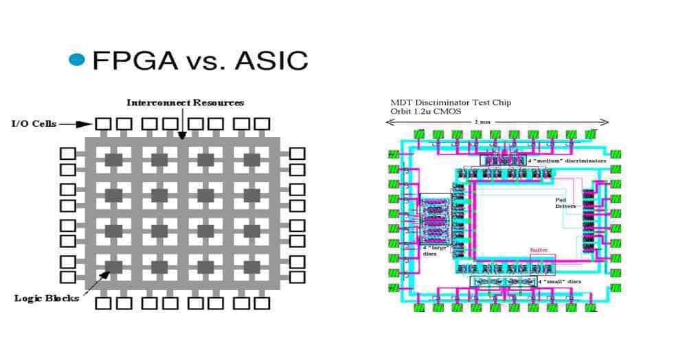
Both Field Programmable Gate Arrays (FPGAs) and Application Specific Integrated Circuits (ASICs) provide the platform upon which components can be configured for onward usage in the targeted applications.
The thin line of difference between the two has to do with the configuration pattern. While the dedicated ASIC chip in ASICs can be used throughout the lifetime of the product or application, unlike the Configurable Logic Blocks (CLBs) in the FPGA, which can be optimized as time goes on.
Therefore, you can regard the FPGA chip as a temporal and fully-reprogrammable component and the ASIC chip as a permanent chip for circuit boards.
Wrapping Up
The overall FPGA PCB design is based on the need to balance the performance of the target applications or consumer electronics. For this to happen, the components (FPGAs) need to be intertwined or interconnected to the board. The best way to do is by verifying the FPGA footprint, implementing the right stackup, implementing the right vendor IP and routing the channels in the right direction.
These all seem technical and that is why you need the services of an experienced FPGA PCB designer. Hillman Curtis has helped hundreds of customers lay the best pathway for their FPGA PCBs, via the use of excellent software. Whether you are looking to design an Altium FPGA, or make the design layout with Allegro or Cadence, we have the capabilities to make that happen. Contact us today.
