Fusion 360 PCB layout is an essential tool for designing printed circuit boards (PCBs). It is a software program that allows you to create and edit PCB designs with ease. Whether you are a professional engineer or a hobbyist, Fusion 360 PCB layout can help you create high-quality PCBs that meet your specific requirements.
One of the key features of Fusion 360 PCB layout is its intuitive user interface. The software is designed to be easy to use, even for those who have little or no experience with PCB design. With its drag-and-drop functionality, you can quickly and easily place components on your PCB and connect them with traces. You can also customize your design by adding text, logos, and other graphics.
Another advantage of Fusion 360 PCB layout is its integration with other tools in the Fusion 360 suite. This allows you to seamlessly move between different design environments, such as mechanical design and electrical design. You can also collaborate with other team members by sharing your designs and working together in real-time. With these features and more, Fusion 360 PCB layout is a powerful tool for anyone looking to create high-quality PCBs.
Getting Started with Fusion 360 PCB Layout
Creating a New PCB Layout
To create a new PCB layout in Fusion 360, you need to start by opening the PCB workspace. You can do this by selecting “PCB” from the dropdown menu in the top left corner of the Fusion 360 interface. Once you have opened the PCB workspace, you can create a new PCB layout by selecting “New PCB” from the “File” menu.
Navigating the Interface
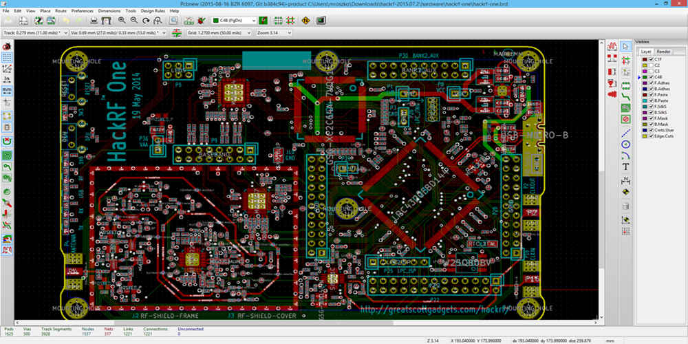
The Fusion 360 PCB layout interface is designed to be intuitive and easy to use. The main window is divided into several panels, including the PCB layout panel, the schematic panel, and the library panel. You can switch between these panels by clicking on the appropriate tab at the bottom of the window.
Setting Up the Design Environment
Before you start designing your PCB layout, you need to set up the design environment to suit your specific needs. This includes configuring the grid and snap settings, selecting the appropriate units of measurement, and setting up the layer stackup for your PCB.
To configure the grid and snap settings, you can use the “Grid and Snap Settings” tool in the toolbar. Here, you can adjust the grid spacing, snap spacing, and other settings to suit your needs.
To select the appropriate units of measurement, you can use the “Units” tool in the toolbar. Here, you can choose between metric and imperial units, as well as adjust the precision of the measurements.
To set up the layer stackup for your PCB, you can use the “Layer Stackup” tool in the toolbar. Here, you can add, remove, and reorder layers as needed to create the desired stackup for your PCB.
By following these steps, you can quickly and easily get started with Fusion 360 PCB layout and start designing your own PCBs.
Designing the PCB Layout

Placing Components
The first step in designing a PCB layout is to place the components on the board. In Fusion 360, you can do this by selecting the components from the schematic and dragging them onto the board. Once placed, you can move and rotate the components to optimize the layout for space and functionality.
It’s important to consider the placement of components carefully, as this can affect the performance of the circuit. For example, placing high-frequency components too far apart can cause signal loss and interference.
Routing Traces
After placing the components, the next step is to route the traces between them. In Fusion 360, you can do this manually or use the autorouting feature to automatically generate the traces.
When routing traces manually, it’s important to ensure that they are as short and direct as possible to minimize signal loss and interference. You should also avoid crossing traces to prevent crosstalk.
Adding Vias
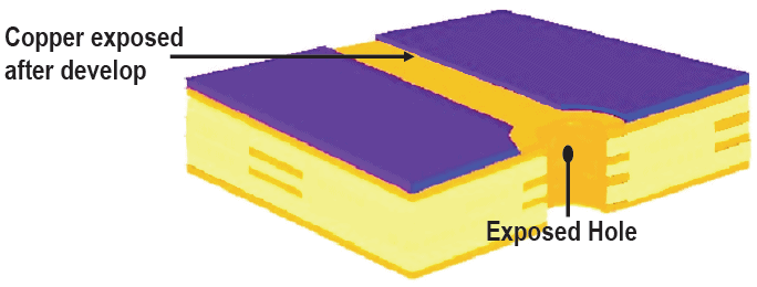
Vias are small holes drilled into the board that allow traces to pass through from one layer to another. In Fusion 360, you can add vias by selecting the trace and clicking on the via icon.
When adding vias, it’s important to consider the size and placement carefully. Vias that are too small can cause signal loss, while vias that are too close together can cause interference.
Adding Pads
Pads are the metal contacts on the board that connect the components to the traces. In Fusion 360, you can add pads by selecting the component and clicking on the pad icon.
When adding pads, it’s important to consider the size and shape carefully. Pads that are too small can cause poor solder connections, while pads that are too large can cause interference.
Overall, designing a PCB layout in Fusion 360 requires careful consideration of component placement, trace routing, via and pad placement. With attention to detail and a clear understanding of the circuit requirements, you can create a functional and efficient PCB layout.
Working with Copper and Layers
Creating Copper Regions
Fusion 360 PCB layout allows for the creation of copper regions, which are used to define the areas on the board where copper will be present. This feature is useful for creating custom shapes and sizes for copper regions, as well as for defining the thickness of the copper.
To create a copper region, select the “Create Copper Region” option from the toolbar. Once selected, you can define the shape and size of the region by clicking and dragging on the board. You can also adjust the thickness of the copper by using the “Copper Thickness” option in the properties panel.
Defining Layers
In Fusion 360 PCB layout, layers are used to define the different components and traces on the board. Each layer can be customized to include specific components or traces, as well as to define the thickness of the layer.
To define a layer, select the “Define Layer” option from the toolbar. Once selected, you can choose the type of layer you want to create, such as a signal layer or a power layer. You can also adjust the thickness of the layer by using the “Layer Thickness” option in the properties panel.
When working with multiple layers, it is important to ensure that the layers are properly aligned and connected. Fusion 360 PCB layout includes a “Layer Stack Manager” feature, which allows you to view and manage the layers in your design.
Overall, working with copper and layers in Fusion 360 PCB layout is a straightforward process that allows for customization and flexibility in your board design.
Generating Manufacturing Files
When you’ve finished your PCB design in Fusion 360, you’ll need to generate manufacturing files to send to your PCB manufacturer. Fusion 360 makes this process easy by allowing you to export Gerber files and create NC drill files.
Exporting Gerber Files
Gerber files are the industry standard for PCB manufacturing. They contain all the information needed to create the copper layers, solder mask, and silk screen on your PCB. To export Gerber files from Fusion 360, follow these steps:
- Go to the “Manufacture” workspace and select “NC Programs” in the “Manufacturing Views” panel.
- Right-click on the “Gerber” folder and select “New Gerber Export.”
- In the “New Gerber Export” dialog box, select the layers you want to include in the Gerber files.
- Choose the output directory and click “OK” to generate the Gerber files.
Creating NC Drill Files
NC drill files are used to create the holes in your PCB. They contain information about the size and location of each hole. To create NC drill files from Fusion 360, follow these steps:
- Go to the “Manufacture” workspace and select “NC Programs” in the “Manufacturing Views” panel.
- Right-click on the “Drill” folder and select “New Drill Export.”
- In the “New Drill Export” dialog box, select the drill file format and units.
- Choose the output directory and click “OK” to generate the NC drill files.
With these manufacturing files, you can send your PCB design to your manufacturer with confidence that it will be fabricated correctly.
Advanced Techniques and Tips
Using Design Rules
One of the most important aspects of creating a successful PCB layout is setting up design rules. Design rules ensure that your board meets the specifications of your manufacturer and that it will function as intended. In Fusion 360, you can set up design rules to control things like trace width, spacing, and clearance. You can also set up rules for different layers, allowing you to create complex designs with ease.
Working with Libraries
Libraries are a powerful tool in Fusion 360 that can save you time and effort. By creating and using libraries, you can easily reuse components across multiple designs and ensure consistency throughout your projects. Fusion 360 includes a number of pre-built libraries, but you can also create your own custom libraries. When working with libraries, it’s important to keep them organized and up-to-date to ensure that you’re using the most current and accurate information.
Utilizing 3D Visualization
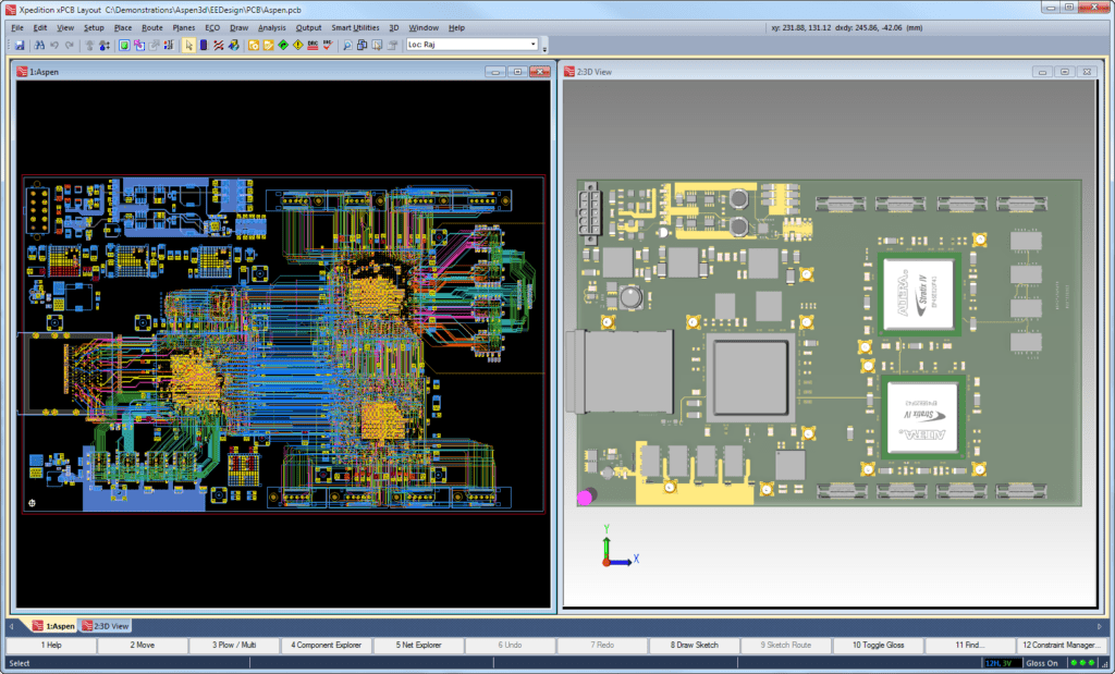
Fusion 360 offers a powerful 3D visualization tool that allows you to view your PCB design in three dimensions. This can be incredibly helpful when trying to visualize how your board will fit into your product or when trying to identify potential issues with your design. By using the 3D visualization tool, you can quickly and easily identify areas that may need adjustment and make changes to your design as needed.
Overall, by utilizing advanced techniques and tips like design rules, libraries, and 3D visualization, you can create more complex and successful PCB layouts in Fusion 360.
