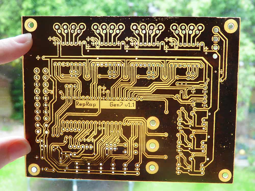
PCB beta layout is a critical step in the process of designing and manufacturing printed circuit boards. The beta layout is the second iteration of the PCB design, following the alpha stage. During the beta layout phase, the design is refined, and any issues or errors identified in the alpha stage are corrected.
The beta layout is an essential step in the PCB design process because it allows engineers to identify and correct any issues before the board is manufactured. This step is crucial because it can save time and money in the long run by preventing costly errors from being made during production. By catching and correcting issues in the beta layout stage, engineers can ensure that the final product will meet all of the necessary specifications and requirements.
Overall, the beta layout is a crucial step in the PCB design process that ensures the final product meets all necessary requirements and specifications. By catching and correcting any issues in the beta layout stage, engineers can save time and money in the long run and produce high-quality PCBs that meet all necessary standards.
What is a PCB Beta Layout?
A PCB Beta Layout refers to the layout design of a printed circuit board (PCB) that is in its beta phase. In other words, it is a prototype of the final PCB design that is being tested and tweaked before it is sent for mass production.
The beta layout is an essential step in the PCB design process as it allows engineers to test the functionality of the circuit and identify any issues or errors that may arise. This stage is crucial as it helps to minimize the risk of costly mistakes during mass production.
During the beta layout phase, engineers may use software tools such as Altium Designer or Eagle PCB to design the layout and simulate the circuit’s behavior. They may also use physical prototyping techniques such as breadboarding to test the circuit’s functionality.
Overall, the PCB beta layout is an important step in the PCB design process that allows engineers to test and refine the circuit’s functionality before it is sent for mass production.
Advantages of Using a PCB Beta Layout
Using a PCB beta layout offers several advantages in the design and manufacturing of printed circuit boards. Here are some of the most notable benefits:
-
Improved Circuit Performance: A PCB beta layout can improve the performance of your circuit by reducing noise, improving signal integrity, and minimizing electromagnetic interference. The layout can also optimize the signal path and reduce crosstalk between traces.
-
Cost Savings: A well-designed PCB beta layout can reduce the number of components required for a circuit. Fewer components mean lower costs for both the components and the board assembly. Additionally, the reduced complexity of the board can lead to faster assembly times, further reducing costs.
-
Ease of Testing and Debugging: A PCB beta layout can make it easier to test and debug your circuit. The layout can provide clear visual cues for identifying components and tracing signal paths, making it easier to locate and diagnose problems.
-
Customizability: A PCB beta layout provides a high degree of customization for your circuit. The layout can be tailored to meet specific design requirements, such as size, shape, and component placement. This flexibility can help you optimize your circuit for performance, cost, and ease of assembly.
-
Improved Reliability: A well-designed PCB beta layout can improve the reliability of your circuit. The layout can reduce the risk of short circuits, improve thermal management, and minimize the impact of environmental factors such as vibration and humidity.
In summary, using a PCB beta layout can improve circuit performance, reduce costs, ease testing and debugging, provide customization options, and improve reliability.
Disadvantages of Using a PCB Beta Layout

While PCB beta layouts can be a useful tool for testing and prototyping, they also come with some significant disadvantages. Here are a few of the most notable drawbacks:
1. Limited Functionality
One of the biggest disadvantages of using a PCB beta layout is that it is typically limited in terms of functionality. Because it is designed primarily for testing and prototyping, it may not have all of the features and capabilities that a production-ready PCB would have. This can be a significant limitation if you need to test a complex system or if you need to test your design under real-world conditions.
2. Increased Cost
Another disadvantage of using a PCB beta layout is that it can be more expensive than other prototyping methods. This is because you will need to purchase the materials and components necessary to create the layout, as well as any specialized equipment that you may need to use. Additionally, if you make any mistakes during the prototyping process, you may need to start over from scratch, which can add to the overall cost of the project.
3. Time-Consuming
Creating a PCB beta layout can be a time-consuming process, particularly if you are new to the process or if you are working with a complex design. You will need to spend time researching and selecting the right materials and components, as well as designing the layout itself. Additionally, you may need to spend time troubleshooting and testing the layout to ensure that it is functioning as intended.
4. Limited Reusability
Finally, it is worth noting that PCB beta layouts are typically not reusable. Once you have created a layout and tested your design, you will likely need to start over from scratch if you want to make any changes or modifications. This can be a significant drawback if you are working on a project with a tight timeline or if you need to make frequent changes to your design.
Overall, while PCB beta layouts can be a useful tool for testing and prototyping, they do come with some significant disadvantages. It is important to carefully consider these drawbacks before deciding whether or not to use a PCB beta layout for your next project.
How to Create a PCB Beta Layout
Creating a PCB beta layout involves several steps that require attention to detail and precision. Here are the steps you can follow to create a PCB beta layout:
-
Start by creating a schematic diagram of your circuit. This will serve as a blueprint for your PCB layout. You can use software like Eagle PCB or Altium Designer to create your schematic.
-
Once you have your schematic, you can begin creating your PCB layout. Start by placing the components on the board. Pay attention to the spacing between components and make sure they are placed in a way that allows for easy routing.
-
After placing the components, you can start routing the traces. Begin by routing the power and ground traces first, then move on to the signal traces. Make sure to avoid crossing traces and keep the traces as short as possible.
-
Once you have completed the routing, you can add any necessary vias and through-holes. Vias are used to connect different layers of the PCB, while through-holes are used to mount components.
-
Finally, you can export your PCB layout to a Gerber file, which is a standard file format used by PCB manufacturers. You can then send the Gerber file to a PCB manufacturer to have your PCB fabricated.
Creating a PCB beta layout requires careful planning and attention to detail. By following these steps, you can create a high-quality PCB layout that meets your circuit design requirements.
Tips for Creating an Effective PCB Beta Layout
When it comes to designing a PCB beta layout, there are several tips that can be helpful in ensuring that the layout is effective and efficient. Here are some tips to keep in mind:
-
Plan the layout before starting: Before diving into the layout, it’s important to have a plan in place. This includes determining the size and shape of the board, the placement of components, and the routing of traces. Taking the time to plan the layout can save time and prevent mistakes later on.
-
Keep it simple: A clean and simple layout is usually the most effective. Avoid overcrowding the board with too many components or traces. Instead, focus on keeping the layout organized and easy to read.
-
Consider the power supply: The power supply is an important aspect of any PCB layout. It’s important to ensure that the power supply is stable and reliable, and that it can handle the load of the components on the board.
-
Use copper pours: Copper pours can be used to connect ground planes and power planes. This can help reduce noise and improve signal integrity.
-
Check for errors: Before finalizing the layout, it’s important to check for errors. This includes checking for short circuits, open circuits, and other common errors.
By following these tips, you can create an effective and efficient PCB beta layout. Keep in mind that designing a PCB layout can be a complex process, and it’s important to take the time to plan and double-check your work to ensure that the final product is of high quality.
Conclusion
In conclusion, PCB Beta Layout is an essential tool for designing and testing printed circuit boards. It allows engineers and designers to create high-quality, reliable, and efficient PCB layouts quickly and easily. By using PCB Beta Layout, designers can reduce the time and cost of PCB design, as well as improve the performance and reliability of their circuits.
One of the most significant advantages of using PCB Beta Layout is its ease of use. It provides a user-friendly interface that makes it easy for designers to create and modify PCB layouts. Additionally, PCB Beta Layout offers a wide range of features and tools that help designers optimize their designs for performance, reliability, and manufacturability.
Another advantage of using PCB Beta Layout is its compatibility with other design tools and software. It can import and export files in various formats, including Gerber, DXF, and IDF. This compatibility makes it easy for designers to collaborate with other team members and share their designs with manufacturers.
Overall, PCB Beta Layout is an essential tool for anyone involved in PCB design and testing. Its ease of use, wide range of features, and compatibility with other design tools make it a must-have for any engineer or designer looking to create high-quality, reliable, and efficient PCB layouts.
