PCB board making is a complex process that involves designing, prototyping, and manufacturing printed circuit boards. These boards are used in a wide range of electronic devices, from smartphones to medical equipment. The process of creating a PCB board involves several steps, including designing the circuit, creating a layout, printing the board, and assembling the components.
One of the most critical steps in PCB board making is designing the circuit. This involves creating a schematic that outlines the connections between components. Once the schematic is complete, the next step is to create a layout that specifies the placement of components and traces on the board. This is a crucial step since the layout can impact the performance of the circuit.
After the design and layout are complete, the next step is to print the board. This involves using specialized software to generate a file that can be used to create a physical PCB board. The board is then fabricated using a variety of techniques, including etching, milling, or printing. Once the board is complete, the final step is to assemble the components onto the board, which can be done manually or using automated equipment.
PCB Board Making Process
Designing the PCB Layout
The first step in making a PCB board is designing the layout using a computer-aided design (CAD) software. The software allows you to create the circuit schematic and place components on the board. The software also helps you to check for errors and optimize the layout for better performance.
Printing the Layout on Copper Board
After designing the PCB layout, the next step is to print it on a copper board using a laser printer. The printer prints the layout on a special transfer paper, which is then transferred to the copper board using a heat press. The heat melts the toner from the transfer paper onto the copper board, creating a resist layer that protects the copper from the etching solution.
Etching the Board
The etching process involves removing the unprotected copper from the board using an etching solution. The solution dissolves the copper, leaving only the traces and pads that form the circuit. After etching, rinse the board with water to remove any remaining etching solution.
Drilling Holes and Placing Components
The next step is to drill holes in the board for the components and connectors. Use a drill bit that matches the size of the components and connectors. After drilling, clean the board to remove any debris or dust. Then, place the components on the board according to the layout.
Soldering Components
The final step is to solder the components to the board. Apply solder to the pads and heat them with a soldering iron. The heat melts the solder, creating a connection between the component and the pad. After soldering, inspect the board for any solder bridges or cold joints.
That’s it! Your PCB board is now ready to be tested and integrated into your project.
Types of PCB Boards

When it comes to PCB boards, there are three main types: single-sided, double-sided, and multi-layer boards. Each type has its own unique characteristics and is suited for specific applications.
Single-Sided PCB Boards
Single-sided PCB boards are the simplest type of PCB board. They consist of a single layer of copper on one side of a substrate material, typically fiberglass or a composite material. The copper layer is etched to create the circuitry, and components are then soldered to the copper traces. Single-sided boards are typically used for simple, low-density circuits, such as those found in calculators and remote controls.
Double-Sided PCB Boards
Double-sided PCB boards have copper on both sides of the substrate material. The circuitry is created by etching both sides of the board, and components are then soldered to the copper traces on both sides. Double-sided boards are used for more complex circuits, and can accommodate a higher density of components than single-sided boards.
Multi-Layer PCB Boards
Multi-layer PCB boards are the most complex type of PCB board. They consist of multiple layers of copper and substrate material, and can have anywhere from four to dozens of layers. The layers are connected by vias, which are small holes drilled through the substrate material and coated with copper. Multi-layer boards are used for high-density circuits, such as those found in computers and smartphones.
In summary, the type of PCB board you choose will depend on the complexity and density of your circuit. Single-sided boards are best suited for simple circuits, while double-sided and multi-layer boards are better suited for more complex circuits.
Materials Used in PCB Board Making
Copper Board
A copper board is the foundation of a PCB. It is a thin layer of copper laminated onto a non-conductive substrate material. Copper boards come in various sizes and thicknesses. The thickness of the copper layer is measured in ounces per square foot (oz/sqft). The most common thickness is 1 oz/sqft. However, thicker copper boards are used for high-current applications.
Soldering Iron
A soldering iron is used to attach components to the copper board. It melts the solder, which creates a bond between the component and the copper board. A good soldering iron should have a temperature control feature, a variety of tips, and an ergonomic handle. A soldering iron with a temperature control feature ensures that the solder melts at the right temperature, preventing damage to the components or the board.
Etching Solution
Etching solution is used to remove the unwanted copper from the board. The board is coated with a layer of photoresist, which is then exposed to UV light through a mask. The exposed areas harden, while the unexposed areas remain soft. The board is then dipped in the etching solution, which dissolves the soft areas, leaving only the copper traces behind.
Drilling Machine
A drilling machine is used to drill holes in the board. These holes are used to mount the components onto the board and to connect the different layers of the board. A good drilling machine should be precise, have a variety of drill sizes, and be able to drill through different materials.
PCB Design Software
PCB design software is used to create the layout of the board. The software allows the user to place the components, route the traces, and generate the necessary files for manufacturing. There are many PCB design software options available, ranging from free to expensive. Some popular options include Eagle PCB, Altium Designer, and KiCad.
In conclusion, these are the essential materials used in PCB board making. Each material plays a crucial role in the manufacturing process, and it is important to choose the right materials for the job.
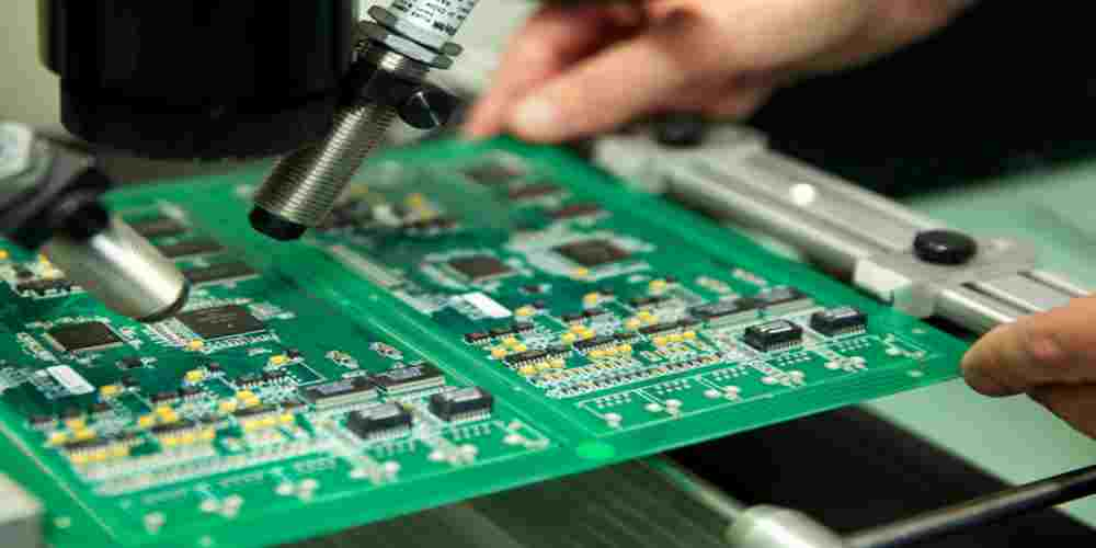
PCB Board Testing
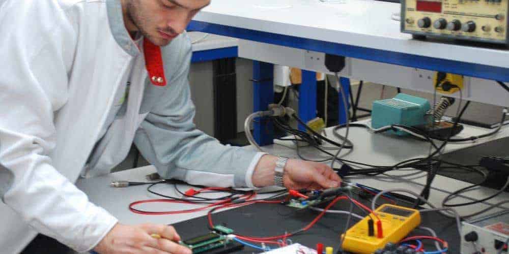
When the PCB board is assembled, it is important to test it to ensure that it is functional and meets the required specifications. There are different types of PCB board testing, including continuity testing, visual inspection, and functional testing.
Continuity Testing
Continuity testing is used to check the connectivity of the circuit on the PCB board. It is done using a multimeter or a continuity tester. The test checks if the electrical current can flow through the board without any interruption. This is important as any interruption in the circuit can cause the PCB board to malfunction.
Visual Inspection
Visual inspection is done to check for any physical defects on the PCB board. This includes checking for any scratches, cracks, or any other damage that may have occurred during the manufacturing process. The inspection is done using a magnifying glass or microscope. Any defects found during the inspection should be documented and addressed before proceeding to the next stage.
Functional Testing
Functional testing is done to check if the PCB board is working as intended. This is done by applying power to the board and checking the output using different types of equipment. The test should be done in a controlled environment to ensure accurate results. Functional testing can be done using different methods, including in-circuit testing, boundary scan testing, and functional testing using a test fixture.
In conclusion, PCB board testing is a crucial step in the manufacturing process. It helps to ensure that the board is functional and meets the required specifications. Continuity testing, visual inspection, and functional testing are the main types of testing used to check the PCB board.
