For circuit board manufacturing, the initial step is that the PCB contract manufacturer reviews the assembly and fabrication data. They are not just verifying all the required data to proceed, they are also searching for any potential problems present in the pcb design which could bring delays or stop the manufacturing. In order to achieve this, some aspects of the pcb design must be examined.
Review of the Bill of Materials
Bill of materials deals with a master list for the parts that are used on your printed circuit board. Also, your PCB contract manufacturer will verify to ensure it matches all the parts utilized in your design. Furthermore, if this BOM has not been updated with recent design information, then it might be outdated.
The next step will be to verify all the components present for the manufacturing. This must be done at a very affordable price or cost. If this doesn’t happen, then your engineering team will advise changes or part substitutions to the design. This will help them make use of the preferred components.
Review of the Design for Manufacturing
Here, we will consider ways in which placing and routing the board’s components are done with respect to manufacturing. Usually, the PCB designs submitted for assembly are not optimized for the process of manufacturing. Also, all these issues will be able to slow down or stop the board assembly.
One good example of this are those parts not placed in line with the solder processes requirements which is used during the assembly. Therefore, it may not solder properly. In addition, the PCB contract manufacturer’s engineering team will get back to you regarding DFM issues that have been discovered during the review. Also, they will give some recommendations on the best ways of resolving the issues.
Review of the Design for Test
Another review to be done is that of the PCB design. This is done for testability. The process is important, and it has to take place at the close of the pcb manufacturing process. This is to verify and ensure that your PCB assembly is completed correctly. Furthermore, it needs the board to feature some test points already built in it coupled with software and test fixtures.
In addition, the engineering team will search for possible areas of improvement in the layout. This is to help enhance the testability and also improve the test coverage. Also, they may alter or build the test fixtures or/and write the test software as required.
Review of the PCB Usability
Asides from the reviews we have already listed, the printed circuit board design will be checked by the engineering team of your contract manufacturer for common issues, which may result in usability issues. For example, the silkscreen reference designators, as well as markings that are incorrect or unclear, or component placement lacking enough space to function in.
In any of these cases, these issues could make using the board very difficult for testing, field technicians, or debugging. Just like all other reviews, all issues discovered will be sent to the customer coupled with possible solutions.
All the reviews above are very important to the manufacturing operation success. These include the expected use and operation of the finished circuit board. Also, if there are any problems, the contract manufacturer’ engineering team will give the customer a full report explaining the issues as well as solutions they recommend. Your engineering team does the work to ensure the circuit board is set for manufacturing.
Preparation for the Circuit Board Assembly: Materials and Component Procurement

After completing the design reviews, the next step of the PCB development process is ordering of the materials and parts. This has to do with everything related to printed circuit boards fabricated raw, electronic components, and sub-assemblies. Immediately you are through with delivering these materials, then the inspection team will start work immediately. They will verify virtually everything that is set for the assembly. Below are the inspection and procurement processes:
Ordering of your bare Boards from the PCB Fabricator
The PCB contract manufacturers usually work with different circuit board fabricators. Some of them specialize in just some PCB technology types. Others on the other hand, might be devoted to just the production of prototype builds.
Having the vendors list, allows the PCB contract manufacturer have the resources to cover the circuit board type.
Immediately you have determined the best possible type for your board type, the fabricator that you have chosen will conduct a DFM review on your design before you proceed. Also, if the review fails to bring up any questions, then they will start the fabrication process. However, if some questions pop up, then the contract manufacturer and the fabricator will work to solve the problem. They will then send back their findings as well as their recommendations to the customer to get an approval.
At times, the times for fabrication have to do with the job’s complexity, and the urgency of the customer. This could take place as early as a few days to a few weeks. The average is usually between five days to one week.
Sourcing and Buying of the Components
Here, the contract manufacturer works on sourcing, buying the components, and other materials necessary. Once the BOM is made clean and there aren’t any problems in the review, the contract manufacturer will first begin with parts already made available in stock, and then they will buy the rest.
Regarding the fabricators of the raw board, the contract manufacturer will have a wide network of manufacturers as well as distributors of components which they work with. This allows the contract manufacturer to find the best delivery tomes and prices for whatever parts they need.
Also, if the BOM has issues with components, which are either expensive, unavailable, or perceived to be obsolete, then the contract manufacturer will respond with respect to at least one of these scenarios.
- Implementing the direct replacement components as well as those that are available from the part manufacturer’s network of the contract manufacturer is usually very easy. The contract manufacturer can go ahead with the substitution after the customer has confirmed it.
- More restrictive component substitution as a result of their availability and function. This requires the contract manufacturer to conduct more research beyond their usual distributor and vendor networks. There are some part brokers, which could be utilized in these scenarios. However the trade off here is that the parts could be costlier or have a shorter life cycle. Before the contract manufacturer proceeds, he or she will contact the customer to discuss any issues and concerns.
- Also, the components will not be available from the broker market or the regular sources of the contract manufacturer because of obsolescence. This leads to discussion with that customer regarding the re-designing options available.
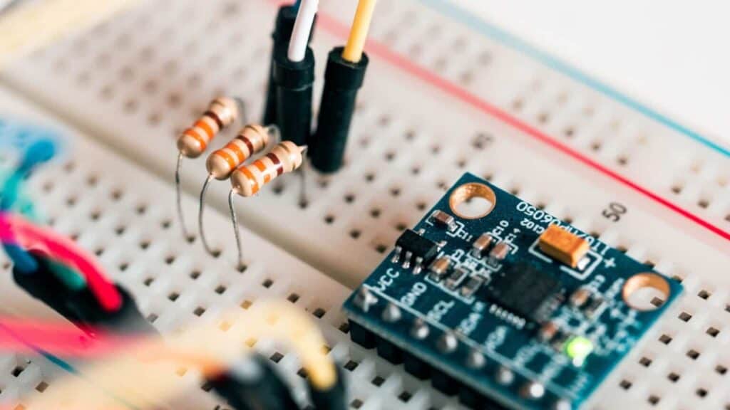
Incoming Inspection for the PCB Assembly Materials and Parts
Immediately the materials, components, and the raw fabricated boards purchased have gotten to your contract manufacturer, they will go through and inspect it before using them in the assembly. These printed circuit boards will also be examined for acceptability and quality before assembling them. This also includes the materials that are used all through the manufacturing process. Furthermore, any ordered sub-assemblies will be inspected to ensure they are manufactured with respect to specifications.
When all the components you have purchased pass through inspection, they are examined. This is for visible damage, cracked cases, broken or bent leads. Also, it includes other issues such as incorrect parts or markings that are outdated.
The testing is conducted with optical equipment to help in enlarging all the parts. The results are then recorded carefully to help in tracking. Though it is impossible to inspect all the components used, your contract manufacturer will perform a sample testing of all the new parts. This comes in till the verification of the component vendor as your trusted supplier.
Furthermore, once the manufacturer has received the ordered materials and parts and inspected them, they’ll go ahead to assign a barcode to them for documentation and tracking purposes. In addition, these materials and parts are pulled together in a kit for its manufacturing floor. After this, your circuit board project will be set for assembly.
Manufacturing Process of the Circuit Board
After you have reviewed as well as verified the design, then the materials and parts have also been ordered and also inspected, then it is time for your manufacturer to create the board. These circuit boards are usually built using a combination of surface mount and thru-hole components.
For each, there are manufacturing steps. First, we will begin with the application of the solder paste which is important for SMT (surface mount components)
Application of the Solder Paste
In contrast to the wave solder whereby the component leads are usually run via a molten solder wave, PCBs which have to be reflowed require the application of solder even before processing them. In order to achieve this, you combine solder flux and metal solder powder. This creates a sticky substance referred to as solder paste.
This solder paste doesn’t just act as a form of temporary adhesive that helps in holding the component leads on the footprint of the circuit board. However, the flex also helps in cleaning up the metal to prepare it for an effective and good solder joint. Furthermore, when this circuit board is made to run through a solder reflow oven, then the paste’s metal particle will melt and then it forms this solder joint.
Usually, the solder paste is applied through screen printing using a jet printer or a stencil. Though setting up and running the jet printing method comes easy, it is usually preferable to make use of the solder stencil. This is because it has the ability to process many circuit boards very quickly.
You can apply solder paste manually using the help of a technician for unique parts or rework. This needs to be soldered by hand. Furthermore, a very significant aspect of the entire process is inspection of the board after applying the solder paste. This makes sure that all the footprints have the right quantity of paste.
Pick and Place Machine
After applying the solder mask, here is a need to install all the components to their appropriate footprints. To perform this operation, you make use of the pick and place machine. These components are all loaded in the machines from trays or reels, and then it is picked up using a vacuum nozzle for the placement.
Making use of the optical alignment equipment for precision, these nozzles move and also rotate the components so as to place them on the footprints.
Furthermore, using automated equipment such as this is usually less expensive. Also, it is much faster in contrast to placing all the parts manually. Some parts like the smaller capacitor packages and resistor, couldn’t be placed manually reliably and then needs the precision of pick and place machines.
Manual Component Insertion
A challenge in building the PCB prototype is the fact that it must fit in the system enclosure prototype, which is usually built with a different manufacturer’s help. Also, contract manufacturers having box build capabilities will be able to manufacture the two projects at once. This makes sure that they work together. With this, it will save you a huge amount of expense and time.
Control Processes and Documentation Generation
Adding to those surface mount components already installed, the majority of circuit boards will have some through hole parts too. Though the surface mount parts are preferable due to their assembly ease, performance, cost, and size there are some important needs, which the thru-hole parts need to supply/. These could include some parts which are useful in very high power appliances, as well as areas whereby part strength is necessary like connectors. In the two cases, the strength and size of the lead which is soldered in the holes offer that part a better advantage.
Soldering Processes of the Circuit Board
Three soldering processes occur during the printed circuit board assembly
Solder reflow
Using the solder paste to hold the surface mount components in place, the printed circuit board is then run on the conveyor belt. The industrial ovens make use of many zones of heat in soldering the board in line with a thermal profile already determined. The programming of the profile in the system is done, thereby allowing the soldering process control by both duration and temperature in different heat zones for the oven.
Wave solder
The through hole parts present on the circuit board has to be soldered making use of the wave soldering machine. This soldering system is true and has been tried and has been used for a very long time in producing circuit boards. These boards are also run via a molten solder wave making use of a specific conveyor system, and this wave then forces the solder in the holes and then around inserted pins. This helps in the forming of a good solder joint. You can even solder some SMT packages like this if a glue holds them in place.
Furthermore, you can set up wave soldering very quickly. It gives a very consistent result than with manual soldering. However, the caveat is, if the board features some areas which cannot travel via the wave, then all these areas have to be prepared beforehand.
Usually, this requires you to create a fixture or mask off areas to protect the features or components present on the board’s bottom from the wave.
Selective Solder
This system is automated and makes use of molten solder that is pumped via a nozzle and used in soldering the thru-hole leads. The system moves in all directions in positioning the leads over that nozzle in line with the way the operator has programmed it.
This system of selective soldering is useful in areas where wave soldering is not effective. This could include components, as well as other board objects, which are too tall and can block the wave, as well as components already soldered and too tight for the protective fixture to be able to fit properly around them.
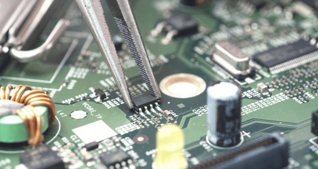
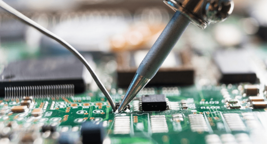
PCBA Rework
Through all the steps that go on during the assembly, the printed circuit board is inspected before you move onto the next step. After the board undergoes automated soldering, this board is inspected again and then the PCBA rework technicians will correct all defects. Asides from assembly defects, this technician can replace the incorrectly specified parts, as well as damaged parts that occurred when reworking the other components.
Circuit Board Test
In order to be sure that the whole assembly process has been finalized and that the printed circuit board will be functioning as expected, the circuit board passes through an automated testing process. Two major methods are applicable for this test. These include the flying probe and in-circuit test, and the two of them rely on testpoints designated when the PCB design is on.
Making use of the test data that has been generated from design files, the test verifies that every component pin is connected strongly using a good solder joint.
Conclusion
After completing the assembly process of the circuit board, this board is then packaged carefully and sent to the customer. This is one good reason why making use of local PCB contract manufacturers pays off. This is because you will not have to face international issues. To develop your PCB, you need to work with the best manufacturer. Choose us today for your PCB development. We will help you understand the benefits you’ll enjoy when you partner with us.
