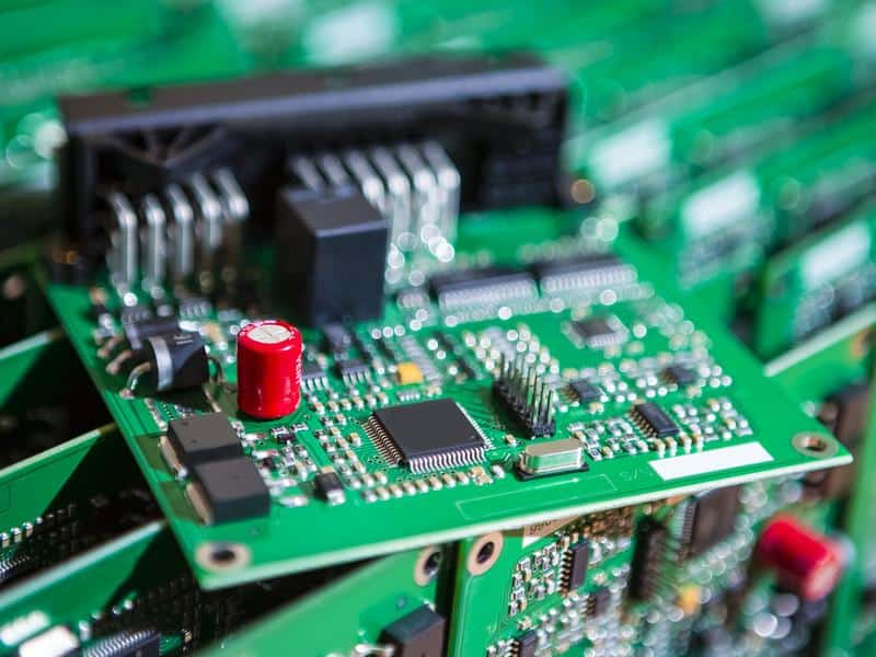
PCB assembly requires a lot of resources and time. Therefore, it is crucial to ensure that the process is quick and efficient to maximize profits and minimize expenses. A PCB assembly company has a range of options to meet your requirements. Take the time to evaluate each company to determine its suitability and responsiveness.
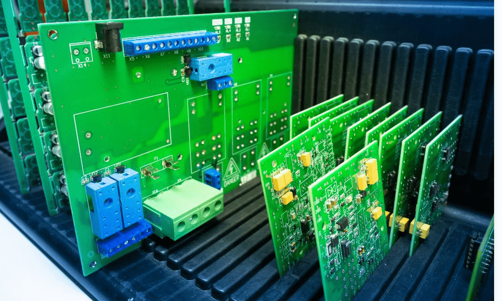
A printed circuit board consists of multiple layers that are all different in functionality. The layers connect through copper lines, which provide an essential purpose for the board to work. In addition, the components link to each other with the help of soldering. As a result, the PCB can be small and thin but perform a complex task. Therefore, it is essential to understand how the components are connected.
Surface-mount technology helps to assemble the majority of PCBs. This technology is faster and more cost-effective than through-hole boards, allowing for higher connection densities. The process also allows for direct mounting of components. Moreover, it is possible to create PCBs that are only one-third the size of a standard through-hole board.
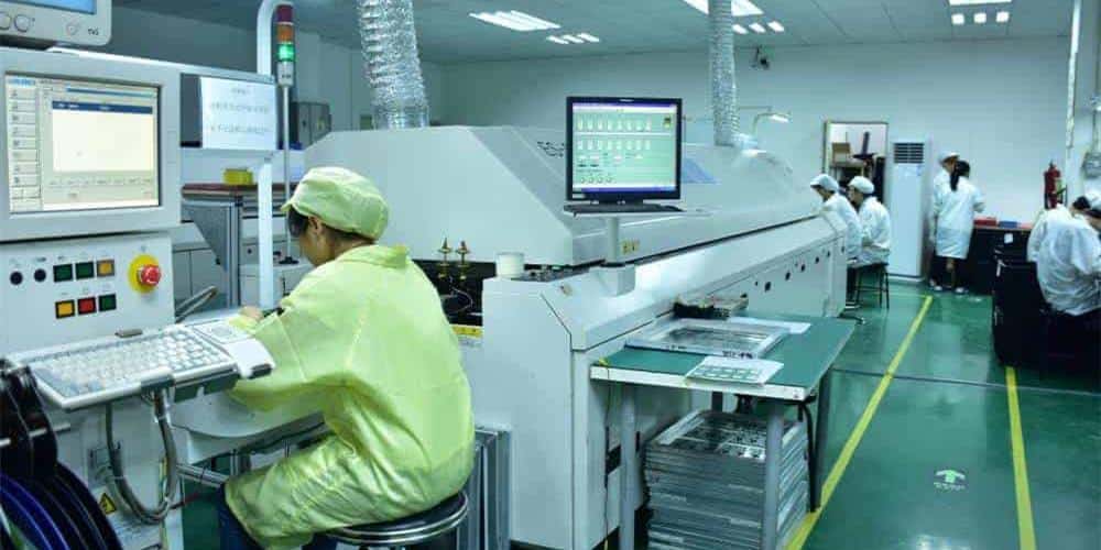
PCB assembly process varies by technology. However, SMT manufacturing is the most common technique used today. The process begins with the programming of a machine. Next, the EMS provider needs the Gerber files of the client to automate the process.
Things to Consider Before PCB assembly process
Before the PCB assembly process, there are several things to consider. Firstly, the PCB assembly enclosure should be a good fit. It should be sturdy and allow easy access to the PCB assembly services. The enclosure should also be easy to clean and maintain. In addition, we must protect PCB assembly against corrosion. Finally, the PCB assembly process should pass a solder paste inspection.
PCB assembly services are easily prone to contamination from various parts of the manufacturing process. For example, flux residue and solder paste residue contain organic acids and ions that can degrade the circuit board. These ions could short circuit your circuit board. Moreover, non-ionic pollutants may penetrate the insulating layer and form dendrites under the PCB surface.
Next, it is essential to understand the assembly process. The PCB assembly process involves several manual and automated steps. In addition, different assembly processes require different procedures.
Therefore, in addition to understanding the basic PCB assembly process, it is also essential to know the different technologies used to manufacture the PCB assembly. Finally, there are specific steps to consider before the PCB assembly process, including a DFM check to evaluate the functionality of the circuit board and its design.
Manual visual inspection is one of the most basic methods of PCB assembly quality inspection. During this process, the operator will use a magnifying glass to check the condition of the PCB assembly process.
The inspector can also check for solder joints that are not fully adhered to each other. Another critical step is inspecting the integrated circuits lead for incomplete welding using a metal needle.
Printed Circuit Board Assembly Design and Manufacturing Process
Regarding PCB assembly Design and Manufacturing, several factors are essential to consider. These factors include AOI (optical inspection), surface finish, and PCB assembly material. These factors help in the production process. Therefore, it is essential to incorporate design decisions into the DFA guidelines to improve efficiency and speed. To do this, you should prepare your design package in the appropriate CM format.
Optical inspection (AOI)
Automatic optical inspection is one of the primary testing processes used in the printed circuit board assembly design and manufacturing process. We can apply it to both bare and assembled boards. The Flying Probe and SMT assembly lines are common examples of automatic optical inspection systems.
An automatic optical inspection machine uses a defined light setting to capture images of a Printed circuit board. The type of lighting used depends on the type of product you are inspecting. Fluorescent lighting is commonly the best. LED lighting is better. AOI systems use image capture and image analysis software to capture an image of the Printed circuit board.
AOI systems compare images of a test circuit board to images of similar boards. The faster an AOI system finds a matched pattern, the faster the inspection process will be. If there is no match, the system will reject the Printed circuit board.
AOI systems can detect short circuits and other issues leading to board failure. They can also detect voids in components and missing pads. We also check the accuracy of the components’ positioning. Automatic optical inspection systems are a must-have for the manufacturing industry.
Automatic optical inspection is one of the essential methods for ensuring the quality of electronic printed circuit boards. Its primary function is to check for defects before they reach consumers. The AOI system uses a camera to take high-definition images of a Printed circuit board.
We can apply the Automatic optical machine at any stage of the fabrication process. However, it is best to do it after reflow soldering since most defects occur during this step.
By identifying defects early, AOI systems can reduce the number of errors and increase inspection efficiency. AOI systems can also help manufacturers optimize their fabrication and assembly process parameters.
Surface finish
There are two primary types of surface finishes used for PCBs. One type uses nickel or gold plating on the copper layer. This finish is applied using a chemical process. It protects the underlying copper from oxidization. The other type uses gold layers to add a barrier to oxidation.
Surface finish selection is essential in the PCB assembly design and manufacturing process. It directly influences the yields, testability, and scrap rates of the Printed circuit board. Therefore, we must consider the assembly process and other considerations to ensure high-quality end products. In addition, the selection process must consider the requirements of different positions in the manufacturing process.
Choosing the surface finish of a Printed circuit board is as critical as selecting the bare board material. The finish must be appropriate for the final application and environment. This final surface finish is crucial to the performance and reliability of the Printed circuit board. Therefore, working with a professional engineer who can help you make the right choice is essential.
When selecting the surface finish, you need to consider the number of functions the Printed circuit board will perform. Each type of finish has its advantages and disadvantages. Fortunately, you can also use engineering tricks to solve surface finish issues. For example, if you don’t like the look of lead plating, you can always switch to an organic surface finish.
The cost of a surface finish is another consideration in the design and manufacturing process. In general, HASL and ENIG are the least expensive. However, they have lower corrosion resistance than other types of surface finish. OSP and HASL are better than other options in terms of ICT.
Printed circuit boards undergo many environmental factors, including dust, moisture, steam, and high temperatures. These conditions can cause copper oxidation.
Printed circuit board material
PCBs consist of three main layers: a conductive layer (usually copper) encased between two layers of dielectric materials. The third layer is the mechanical layer, which we apply after gluing the other two layers together. Finally, we cover the copper trace exposed on some PCBs with a solder mask to prevent corrosion.
After making the printed circuit boards, the outer layer undergoes a series of processes to ensure they align with design specifications. For example, a process known as solder mask application involves applying epoxy solder ink to the surface of a printed circuit board. Afterward, we subject the printed circuit board to an automated optical inspection process. Lastly, we cure the solder mask under UV light.
The materials used in a Printed circuit board are critical to the electrical performance of the board. The substrate material determines the circuit board’s frequency sensitivity. This frequency dependence introduces phase distortion into wideband applications, and the transmission line impedance decreases with frequency. This makes fast-moving edges of signals reflect more strongly than slower ones. In addition, the dielectric breakdown voltage of the material determines how much voltage it can withstand, and the tracking resistance shows how much resistance it can stand up to high voltage discharges creeping over the board surface.
The PCB fabrication process begins with the creation of blueprints, which are generally completed by computer software. In this phase, the design process begins with the circuitry layout, with the first layer containing conductive copper traces. Next, the second layer of the Printed circuit board goes through a second check referred to as the Design for Manufacture (DFM). This stage ensures that all components are connected correctly and meet tolerance requirements. Once the PCB design is complete, the design goes through a printing phase to finish the board.
Laser printing
LDI is a new process that uses lasers to print circuitry images directly onto Printed circuit board panels. It eliminates the need for photo tools and is far more precise than conventional film printing methods. It also eliminates the need to recreate photo tools regularly. This process is more expensive than traditional photolithography but provides improved accuracy, resolution, and perfect alignment.
Before fabricating circuit boards, they undergo a Design for Manufacture check to ensure that their circuits meet design and manufacturing specifications. We then print the PCBs using plotter printers. These plotters use an exact printing process to create a photo film of the circuit boards.
Another process, called laser etching, involves the removal of copper directly from the board. This is helpful for prototyping. However, the amount of copper removed depends on the number of boards produced and the resolution required. Another method, known as laser printing on resist, involves laser-printing the resist onto toner transfer paper, heat transfer, and touch-up. Other methods, including non-washable markers and vinyl film, are also used.
Traditionally, we design PCBs by creating a photomask on a clear mylar sheet, which is two to four times true size. Then, we routed traces to connect the component pin pads. Often, the photomask was then photolithographically reproduced onto blank copper-clad boards. During the process, the designer would use the electronic design automation (EDA) tool to capture the schematic. The PCB CM would then choose a Printed circuit board fabricator to fabricate a prototype for the design review. Therefore, selecting a Printed circuit board fabricator who can produce a prototype is essential. In addition, this vendor should have its production line and must conduct design reviews using Gerber data.
Things to Consider After the Printed circuit board Assembly Process
The PCB assembly process begins with the THT components being placed on the circuit board and soldered together. We do this using a wave soldering system that works at 500degF. Next, the board moves to another station, where the next person inserts a different PTH component.
The PCB is now ready for the final inspection. The testers will simulate how the PCB works and record the electrical characteristics. If the test passes, the PCB can move on to the next step. This step is known as the “functional test” because it simulates a typical PCB’s operation.
The assembly process can be manual or automatic. First, the designer creates a file for the automated robot that includes preprogrammed X and Y coordinates for each component. The robot will then place the components on the PCB. Surface mount components make up most of the components on PCBs today.
After the PCB assembly process is complete, the soldering process can begin. We can do the PCBA process with various materials, including metal, epoxy glass, and resin. Some PCB assembly processes also use surface-mount devices, which are common in high-tech applications. However, regardless of the type of board, we must perform a soldering process at some point in the manufacturing process.
PCB Layers and Design
Before deciding on PCB layers and design, it is vital to determine the board’s purpose. This will determine how many layers are required, the type of machine used, and the complexity of the electronic circuit. The number of layers can also be affected by the power requirements. High-tech applications usually require more layers.
Prepreg sublayer
Prepreg is a crucial component of the Printed circuit board assembly. This composite material, which consists of fiberglass impregnated with resin, is used to hold the layers together on a PCB. A single piece of this material can hold up to four layers, and it helps the board’s layers and design adhere together.
The inner layer of a four-layer PCB consists of two 0.0091-inch-thick sheets. The bottom layer is 0.0014-inch-thick and serves as the signal layer. We solder interconnects on the top and bottom layers. This method ensures that the boards are safe and reliable and will last a long time. The two inner layers consist of copper.
We cover the copper circuitry with a multilayer FR-4 prepreg, a flame-retardant sheet of fiberglass with no copper foil cladding. This composite is pressed at low temperatures and is helpful for high-frequency applications. In addition to a single layer of pre-laminated copper, multilayer boards may have one or more etched or printed layers.
Signal layer
The signal layer on a Printed circuit board assembly identifies multiple signals and components. Unlike the component layer, which shows only one signal, we can break up the signal layer to represent multiple plane signals. It is an effective way to separate a ground plane from an adjacent signal line. Therefore, the signal layer is an essential part of a PCB design.
The signal layer comprises copper traces etched onto a dielectric layer. These traces form the circuitry of your design. Finally, the power/ground layer is composed of a solid copper plane.
Net layer
The Net layer is a crucial design component that helps separate the traces. Nets can be grouped into classes, depending on their size and the desired routing. For example, trace length, width, and spacing can define a class. In addition, certain types of nets may have specific routing requirements, such as timing and impedance.
Nets that support high-speed signal transmission have different trace width requirements, and their layers may have specific restrictions. They also may need narrow traces in dense areas called necking down. This is often necessary for devices with high-pin counts. This layer is often on the top surface of the board.
The Net layer is common in Printed circuit board assembly. It helps to provide power and stability to the components on the board.
Bottom layer
The PCB design process has the Top Overlay layer, Bottom Overlay layer, and Mechanical Layer. The Top Overlay layer identifies and labels components and their projection profiles. The Bottom Overlay layer, on the other hand, identifies and labels exposed surface mount pads. These pads need coating with solder paste before welding. On the other hand, mechanical layers are essential for hot-air leveling pads and welded stencils.
The Bottom layer of the Printed circuit board assembly consists of several electronic components. The board outline is the top layer, which is usually the signal layer. This layer consists of 0.0014-in.-thick copper, which weighs about a gram. It impacts the final thickness of the board, which is usually 0.062 inches. However, the copper thickness may vary depending on the board fabrication parameters.
Keep out layer
A keep-out layer is a useful tool to protect interior segments of a Printed circuit board assembly from external interference. Keep-outs can be helpful for mechanical reasons as well as aesthetic purposes. They help limit the working space of the board, especially near mounting holes. Therefore, the keep-out layer is essential to PCB design.
The solder paste layer is typically on the solder paste layer, but some designers do not include it on the physical PCB. The reason for this is that it makes the assembly process easier. When creating your PCB, use a Bill of Materials (BOM) to list the components’ names and values.
Types of PCB electronic Assembly Mounting Technology
There are several types of PCB assembly mounting technology available. Using the right type of technology depends on the PCB design and reliability requirements. For example, surface-mount technology is widely essential for assembling printed circuit boards, as it does not require drilling holes in the PCB. This type of mounting involves picking and placing electronic components on bare boards.
Surface-mount components
The advantages of surface-mount components for electronics PCB assembly include reduced production cost and ease of assembly. It also allows the manufacturing of high-performance circuits in small packages. In addition, unlike through-hole technology, surface-mount technology (SMT) can produce circuits with higher component density per unit area. As a result, it is the industry standard for electronic assembly and PCB manufacturing.
The components are smaller and more reliable when using surface-mount technology (SMT) for PCB assembly. In addition, these electronic components are easier to place using automatic pick and place machines. In contrast, wire components are challenging to place automatically because we must perform them to match the holes and are prone to errors during placement. Some PCB components still require manual placement, but this number has declined over the years.
Through-hole technology
There are several benefits of through-hole technology for PCB assembly mounting. The first is the reduction of space. Compared to traditional assembly methods, through-hole technology allows for a remarkably compact board. As a result, through-hole components can dramatically reduce the area of a PCB. However, the technique is still relatively uncommon. Consequently, through-hole is only helpful in a small number of products.
Another benefit of through-hole technology is the reduction of assembly time. This type of mounting can simplify small-lot production and prototyping. In addition, through-hole components are ideal for early validation and development. As a result, through-hole technology may be a good choice for electronics start-ups, hobbyists, and established electronics suppliers.
Mixed technologies
When designing a PCB, there are several different PCB assembly mounting technologies that are available. The first one, surface mount technology, uses the PCB’s two sides and is faster than through-hole assembly. The other is through-hole assembly, which uses pre-drilled holes and requires significant, incompatible electronic components. A hybrid technique combines these two types of mounting technologies.
Mixed technologies for PCB assembly mounting combine the advantages of each type of technology. This method involves passing a PCB assembly through the preheat and soldering process. First, the PCB is mounted on a conveyor and runs through a heating chamber. Next, this method applies solder paste to all the underpins of the board in one process.
Benefits
Reliability
The reliability of PCB assembly mounting technology is an essential aspect of PCB manufacturing. Many things can go wrong during the assembly process, so choosing the right technology is imperative to avoid such problems. The first thing to consider is minimizing the number of metalized holes and connectors on the board. This can help minimize the risk of poor contact between the electronic components on the board and other parts. The next thing to consider is the temperature of the devices on the board. Extreme temperatures can reduce their performance, so thermal protection measures should help minimize the devices’ temperature and ensure good heat dissipation. These measures will increase the reliability of the equipment.
Surface-mounted technology (SMT) has many benefits. It can reduce the size of PCBs while maintaining the same component density. In addition to the size savings, SMT also offers higher reliability due to fewer drilling holes. It also offers faster production times. SMT can place thousands of electronic components per hour, whereas THM can only place a few hundred per hour. It is also more stable than THT and has been proven more reliable even under shaking and vibration. But it’s important to remember that SMT requires advanced production and design skills.
Cost
Many factors can affect the cost of PCB assembly. The complexity of the design, labor rates, and overhead expenses can all affect the price. The time it takes for Printed circuit board assembly can also influence the cost. Complex designs are more challenging to assemble, so the more difficult they are, the more they will cost. Several methods are available to reduce the overall cost of electronics PCB assembly.
Surface mount technology is the least expensive PCB assembly method. Surface-mounted electronic components are also lighter and smaller, often faster and more powerful than their through-hole counterparts. Through-hole technology, however, requires drilling holes in the PCB and installing components.
Solder Paste in the PCB Assembly Process
When we use solder paste in the PCB assembly process, it is essential to follow specific procedures. These steps include proper cleaning of the paste after soldering. In addition, one should store the paste in a properly ventilated area with a large surface area. Also, we must store solder paste at low temperatures to minimize oxidation and flux degradation.
First, you heat the paste in a heating channel. The heating channel has two main sections: preheating and active zones. The first one occupies approximately 25-thirds of the entire length. The second one occupies the remaining 25-33%. The preheating zone is essential to the PCB assembly process because it helps raise the PCB temperature from ambient to active. If the temperature rises too fast, it can lead to defects in the capacitors and solder paste. On the other hand, if the preheating zone is too slow, the PCB may not reach its active temperature promptly.
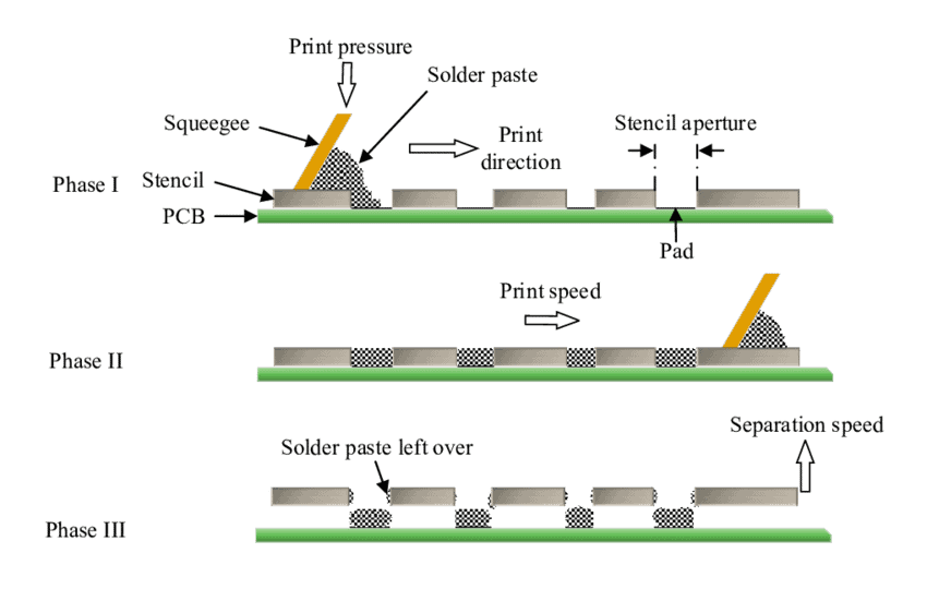
Solder paste application
The application of solder paste requires accurate stencils. If the stencils are not accurate, they will hinder the application of the paste. The process also involves the use of metal and mesh screen printing. Although metal screen printing is less expensive, mesh screen printing is more suitable for smaller surface mount devices. In addition, a quality solder paste application will ensure the board’s integrity.
Solder paste is a necessary part of the PCB assembly process. It acts as a bond between the electronic components and the PCB. The solder paste application process will vary depending on the type of soldering.
A squeegee blade is the most common method for applying solder paste to a PCB. The blade applies force to the solder paste and can consist of metal or polyurethane. The speed at which the squeegee moves determines how long the solder paste will roll across the surface.
Solder paste is a mixture of tiny solder particles and flux. It is grey, and we apply it to the PCB’s pads and leads. The paste is then heated and melted to connect the electronic components. The paste should be free of contaminants.
The solder paste application process is a tedious task. There are different squeegees for each type of electronic component. Some squeegees help apply solder paste to dense-footed components, while others are essential for standard surface mount pads. The amount of solder paste used varies widely for both types of features. The thickness of the pads is another factor that affects the amount of solder paste used.
Wave Soldering for PCB Assembly
Wave soldering is the process of joining the electronic components on a PCB. This process has two primary defects: pinhole defects and blowhole defects. Both are related to the thickness of the copper plating on the board. Pinhole defects result from excess moisture from the board oozing through the thin plating, forming holes.
The wave soldering process is a two-step process. First, the assembly enters the solder wave. Wave soldering accommodates up to half of the PCB thickness and flows at the same speed as the assembly. The assembly then leaves the wave at the flat crest. As the solder flows over the PCB, it displaces the solder from the front of the wave. This separation prevents the solder from oxidizing.
Wave soldering also involves cooling the PCB and components during the process. The wave soldering process consists in adjusting the flux and solder applied to the electronic component bodies. This process was time-consuming, expensive, and required constant maintenance.
Then, the PCB assembly had to undergo another step to cure the glue. This process needed UV curing and additional equipment. Finally, achieving the right balance between the PCB and the components was difficult.
Wave soldering is a great option for large power devices and high pin-count connectors. In addition, it is an excellent way to ensure the fidelity of the connections. Wave soldering is also a great choice for PCBs with multi-lead electronic components.
