Printed circuit board (PCB) computer-aided design (CAD) is a vital tool for designing and manufacturing electronic devices. PCB CAD software allows designers to create schematics and layouts for printed circuit boards, which are then used to manufacture the boards. The software also provides tools for testing and troubleshooting the design, ensuring that the final product meets the required specifications.
PCB CAD software has revolutionized the way electronic devices are designed and manufactured. With the ability to create complex designs quickly and accurately, PCB CAD software has made it possible for companies to bring new products to market faster than ever before. The software also allows for easy collaboration between designers and manufacturers, reducing the time and cost involved in bringing a product to market. Additionally, PCB CAD software has made it possible for smaller companies and individuals to design and manufacture electronic devices, leveling the playing field in the industry.
Overview
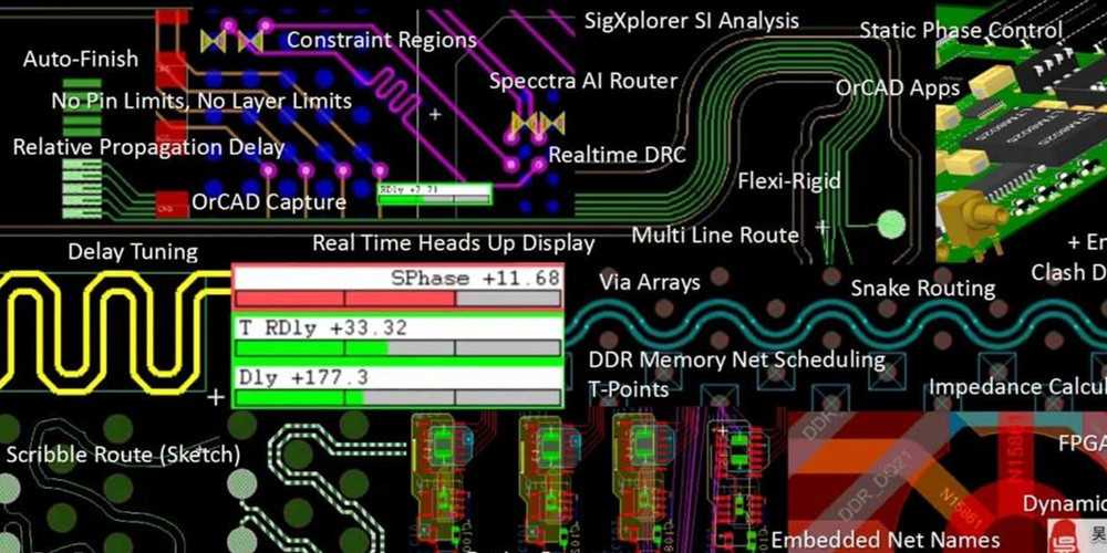
Printed Circuit Board CAD, or PCB CAD, is a software tool used by electronic engineers to design and develop printed circuit boards. PCB CAD software allows engineers to create a virtual representation of a circuit board, including all of its components, traces, and other features. This virtual representation can then be used to manufacture the actual circuit board.
PCB CAD software typically includes a wide range of features and tools to help engineers design and develop circuit boards. These tools may include schematic capture, layout design, autorouting, design rule checking, and more. Some PCB CAD software may also include simulation capabilities, allowing engineers to test their designs before manufacturing them.
One of the key benefits of using PCB CAD software is that it allows engineers to quickly and easily iterate on their designs. Because the software provides a virtual representation of the circuit board, engineers can make changes and modifications to the design without having to physically prototype the board. This can save a significant amount of time and resources.
Another benefit of using PCB CAD software is that it can help ensure the accuracy and reliability of the final circuit board. By using design rule checking and other features, engineers can identify potential issues and errors in the design before it is manufactured. This can help prevent costly mistakes and ensure that the final circuit board meets the necessary specifications and requirements.
Overall, PCB CAD software is an essential tool for electronic engineers who are involved in the design and development of printed circuit boards. With its wide range of features and capabilities, PCB CAD software can help engineers create accurate, reliable, and high-quality circuit board designs in a timely and cost-effective manner.
Benefits

Printed circuit board CAD comes with a variety of benefits that make it a popular choice for designing and manufacturing electronic devices. Here are some of the most significant benefits:
Time-Saving
One of the most significant benefits of using PCB CAD software is that it saves time. With PCB CAD software, designers can create and modify designs quickly and easily. The software’s intuitive interface and automation capabilities make it easy to create accurate and error-free designs in a fraction of the time it would take to manually draw them.
Cost-Effective
PCB CAD software is also cost-effective. By using PCB CAD software, designers can eliminate the need for expensive physical prototypes. Instead, they can create virtual prototypes and test them in a simulated environment. This not only saves time but also reduces the cost of manufacturing.
Improved Accuracy
PCB CAD software also improves accuracy. With the software’s advanced design tools and simulation capabilities, designers can create highly accurate and error-free designs. This reduces the risk of errors and ensures that the final product meets the required specifications.
Enhanced Collaboration
PCB CAD software also enhances collaboration between designers and manufacturers. With the software’s cloud-based design tools, designers and manufacturers can work together in real-time, regardless of their location. This speeds up the design process and ensures that everyone is on the same page.
Scalability
Finally, PCB CAD software is highly scalable. It can be used to design and manufacture electronic devices of all sizes, from small consumer products to large industrial equipment. This makes it an ideal choice for businesses of all sizes, from startups to large corporations.
In conclusion, PCB CAD software offers a range of benefits that make it an essential tool for designing and manufacturing electronic devices. From time-saving to improved accuracy, enhanced collaboration, and scalability, PCB CAD software has something to offer everyone.
Design Process

The design process for printed circuit board (PCB) CAD involves several steps that are critical to ensure the final product is functional and meets all requirements. Here are the key steps involved in the design process:
-
Schematic Capture: This is the first step in the design process, where the circuit schematic is created using a CAD tool. The schematic capture tool allows designers to create a visual representation of the circuit, including the components and their connections.
-
Component Placement: Once the schematic is created, the next step is to place the components on the PCB. The placement of components is critical to ensure that the PCB is compact and efficient. The CAD tool provides a feature to automatically place the components, or designers can manually place them.
-
Routing: After the components are placed, the next step is to route the connections between them. This involves selecting the appropriate trace width, spacing, and layer for each connection. The CAD tool provides a feature to automatically route connections, or designers can manually route them.
-
Design Rule Check (DRC): Once the routing is complete, the CAD tool performs a DRC to ensure that the design meets all the requirements. The DRC checks for errors such as overlapping traces, incorrect trace width, and incorrect spacing.
-
Gerber Generation: The final step in the design process is to generate the Gerber files. Gerber files are the industry-standard format for PCB manufacturing. The CAD tool generates the Gerber files, which are then sent to the PCB manufacturer for manufacturing.
In conclusion, the design process for PCB CAD involves several critical steps that are necessary to ensure the final product is functional and meets all requirements. The CAD tool provides several features that make the design process efficient and accurate.
Tools and Software

Printed circuit board (PCB) design requires specialized software and tools to create the necessary schematics and layouts. Here are some of the most commonly used tools and software in the industry:
Schematic Capture Tools
Schematic capture tools are used to create the electrical circuit diagram that will be used in the PCB design. Some of the most popular schematic capture tools in the market include:
- Altium Designer
- Eagle PCB Design
- KiCAD
- Proteus PCB Design
PCB Layout Tools
PCB layout tools are used to create the physical layout of the circuit board. These tools allow designers to place components, route traces, and generate Gerber files for manufacturing. Some of the most popular PCB layout tools in the market include:
- Altium Designer
- Eagle PCB Design
- KiCAD
- OrCAD PCB Designer
- PADS PCB Design
Simulation Tools
Simulation tools are used to test the circuit design before it is manufactured. These tools allow designers to simulate the behavior of the circuit under different conditions and identify potential issues. Some of the most popular simulation tools in the market include:
- LTSpice
- PSpice
- Proteus PCB Design
Manufacturing Tools
Manufacturing tools are used to generate the necessary files for the manufacturing process. These tools include:
- CAM350
- GC-Prevue
In conclusion, the PCB design process requires specialized software and tools to create schematics, layouts, and manufacturing files. The industry-standard tools include Altium Designer, Eagle PCB Design, KiCAD, and Proteus PCB Design. Simulation tools such as LTSpice, PSpice, and Proteus PCB Design are used to test the circuit design before manufacturing. Finally, manufacturing tools such as CAM350 and GC-Prevue are used to generate the necessary files for the manufacturing process.
