Printed circuit board (PCB) layout design is an essential part of the electronics industry. PCBs are used in almost every electronic device, from smartphones to computers, and are responsible for connecting and controlling the various components of a device. The layout of a PCB can greatly affect the performance and reliability of a device, making it a crucial aspect of electronic design.
PCB layout design involves arranging the components and interconnecting traces on a board to ensure proper functionality and signal integrity. The layout must also consider factors such as heat dissipation, electromagnetic interference, and manufacturability. With the increasing complexity and miniaturization of electronic devices, PCB layout design has become more challenging and requires specialized knowledge and software tools.
In this article, we will explore the basics of PCB layout design, including the key considerations and techniques used in the process. We will also discuss the importance of proper PCB layout design and the impact it can have on the overall performance and reliability of electronic devices.
Basics of Printed Circuit Board Layout
Printed Circuit Board (PCB) layout is the process of designing and arranging electronic components on a PCB to ensure that the circuit functions as intended. The layout of a PCB plays a critical role in determining the performance and reliability of the circuit.
The basic principles of PCB layout include:
Component Placement
The placement of components on a PCB should be done in a way that minimizes the length of the conductive traces between them. This helps to reduce the resistance and inductance of the traces, which can improve the performance of the circuit. Components should be placed in a logical and organized manner, with consideration given to the location of power and ground connections.
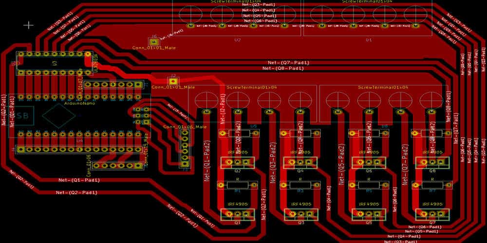
Trace Routing
Trace routing involves connecting the various components on the PCB with conductive traces. The routing of traces should be done in a way that minimizes the length of the traces and avoids crossing over each other. This helps to reduce the capacitance and crosstalk between the traces, which can improve the signal integrity of the circuit.
Power and Ground Planes
Power and ground planes are large areas of copper on the PCB that provide a low impedance path for the flow of current. These planes help to reduce the noise and interference in the circuit and improve the power delivery to the components.
Signal Integrity
Signal integrity is a measure of the quality of the signal as it travels through the PCB. The layout of the PCB can have a significant impact on the signal integrity of the circuit. Factors that can affect the signal integrity include the length and routing of the traces, the placement of components, and the use of power and ground planes.
In summary, PCB layout is a critical aspect of electronic circuit design. A well-designed layout can improve the performance and reliability of the circuit, while a poorly designed layout can lead to problems such as noise, interference, and signal degradation. By following the basic principles of PCB layout, designers can create circuits that meet their performance and reliability requirements.
Factors to Consider in Printed Circuit Board Layout

Printed Circuit Board (PCB) layout is a crucial aspect of electronic design. It involves the arrangement of components, traces, and other elements on a board to ensure proper functioning of the circuit. Here are some factors to consider when designing a PCB layout:
-
Component Placement: The placement of components on the board is crucial for efficient circuit operation. Proper placement of components can reduce noise and interference, improve signal integrity, and minimize the length of traces.
-
Trace Routing: The routing of traces is another important aspect of PCB layout. The routing of traces must be done in a way that minimizes interference and noise. Traces should be kept as short as possible, and high-speed signals should be routed on inner layers to reduce crosstalk.
-
Power and Ground Planes: The use of power and ground planes can significantly improve the performance of a circuit. These planes provide a low impedance path for current flow and help to reduce noise and interference.
-
Signal Integrity: Signal integrity is critical for the proper functioning of a circuit. Proper PCB layout can help to ensure signal integrity by minimizing the length of traces, reducing crosstalk, and controlling impedance.
-
Thermal Considerations: Thermal considerations are important to ensure that the PCB operates within the required temperature range. Adequate spacing between components, proper use of thermal vias, and the use of copper pours can help to dissipate heat and improve thermal performance.
In conclusion, PCB layout is a critical aspect of electronic design that must be carefully considered. Proper component placement, trace routing, power and ground planes, signal integrity, and thermal considerations can all significantly impact the performance of a circuit.
Designing Printed Circuit Board Layout
Designing a printed circuit board (PCB) layout is a crucial step in the process of creating a functional electronic device. The PCB layout determines the physical arrangement of components, traces, and other elements on the board. A well-designed PCB layout can ensure that the device operates efficiently and reliably.
When designing a PCB layout, it is important to consider the following factors:
-
Component placement: Components should be placed strategically to minimize the length of traces and reduce the risk of interference.
-
Trace routing: Traces should be routed in a way that minimizes their length and reduces the risk of crosstalk and other forms of interference.
-
Power and ground planes: Power and ground planes should be designed to provide a stable power supply and minimize noise.
-
Signal integrity: Signal integrity should be maintained by minimizing the length of traces and reducing the risk of interference.
-
Thermal management: Thermal management should be considered to ensure that components do not overheat and malfunction.
To aid in the design process, many software tools are available to help with PCB layout. These tools can help with component placement, trace routing, and other aspects of PCB design.
In summary, designing a PCB layout is a critical step in the process of creating a functional electronic device. By considering factors such as component placement, trace routing, power and ground planes, signal integrity, and thermal management, a well-designed PCB layout can ensure that the device operates efficiently and reliably.
Tools and Software for Printed Circuit Board Layout
When it comes to designing printed circuit boards, having the right tools and software can make all the difference. Here are some of the most commonly used tools and software for printed circuit board layout:
1. PCB Design Software
PCB design software is essential for creating the layout of a printed circuit board. Some of the most popular PCB design software include:
- Altium Designer
- Eagle PCB Design
- KiCAD
- OrCAD PCB Designer
- PADS PCB Design
Each software has its own strengths and weaknesses, so it’s important to choose the one that fits your needs and budget.
2. Schematic Capture Software
Schematic capture software is used to create the schematic diagram of the circuit that will be laid out on the printed circuit board. Some of the most popular schematic capture software include:
- Altium Designer
- Eagle PCB Design
- KiCAD
- OrCAD Capture
- PADS Logic
3. PCB Layout Design Rules Checker
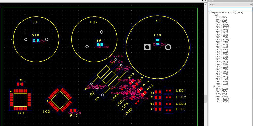
A PCB layout design rules checker is a software tool that checks the layout of the printed circuit board against a set of design rules. This ensures that the board will function as intended and that there are no errors in the layout. Some of the most popular PCB layout design rules checker include:
- Altium Designer
- Eagle PCB Design
- KiCAD
- OrCAD PCB Designer
- PADS PCB Design
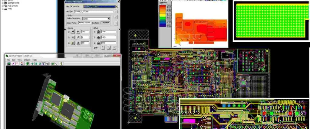
4. 3D Modeling Software
3D modeling software can be used to create a 3D model of the printed circuit board, which can be useful for visualizing the final product and identifying any potential issues. Some of the most popular 3D modeling software include:
- Altium Designer
- Eagle PCB Design
- KiCAD
- SolidWorks
- AutoCAD
Overall, having access to the right tools and software can greatly improve the efficiency and accuracy of printed circuit board layout.
Tips and Best Practices for Printed Circuit Board Layout
When designing a printed circuit board (PCB), there are a few tips and best practices that can help ensure a successful outcome. These tips and practices include:
-
Plan ahead: Before starting the layout, make sure you have a clear understanding of the requirements and constraints of the design. This includes the size and shape of the board, the number of layers, the placement of components, and the routing of traces. Planning ahead will help prevent costly mistakes and ensure that the design meets the necessary specifications.
-
Keep it simple: Avoid overcomplicating the design by using too many layers, vias, or components. This can lead to signal integrity issues, increased cost, and decreased reliability. Instead, aim for a simple and elegant design that meets the necessary requirements.
-
Follow design rules: Most PCB design software includes design rule checks (DRCs) that help ensure that the layout meets certain requirements. These rules include minimum trace widths, clearances, and via sizes. Following these rules can help prevent errors and ensure that the design is manufacturable.
-
Minimize noise: Noise can be introduced into the design through a variety of sources, including power supplies, clocks, and other components. To minimize noise, keep high-speed traces as short as possible, use decoupling capacitors, and separate sensitive components from noisy ones.
-
Test early and often: Testing the design early in the process can help identify issues before they become major problems. This includes testing for signal integrity, power integrity, and thermal issues. Testing often throughout the design process can help ensure that the design meets the necessary requirements and can be manufactured successfully.
By following these tips and best practices, designers can create successful and reliable PCB layouts that meet the necessary specifications.
