SMD PCB layout is an essential aspect of modern electronics manufacturing. Surface mount technology (SMT) has revolutionized the industry by reducing the size of components and increasing the efficiency of the manufacturing process. SMD PCB layout is the process of designing the placement of components on a printed circuit board (PCB) using surface mount technology.
SMD PCB layout has become increasingly popular due to its many advantages over traditional through-hole technology. SMT components are much smaller than their through-hole counterparts, allowing for higher component density on a PCB. This leads to smaller and lighter devices with improved performance. Additionally, SMT components can be placed and soldered using automated equipment, resulting in faster and more efficient manufacturing processes.
Basics
What is SMD PCB Layout?
Surface Mount Device (SMD) PCB layout is a method of designing and assembling electronic circuits that uses small, surface-mounted components instead of traditional through-hole components. SMD components are mounted directly onto the surface of the printed circuit board (PCB) and soldered in place using a reflow oven or a soldering iron.
SMD PCB layout is becoming increasingly popular due to its many advantages over traditional through-hole components. SMD components are smaller, lighter, and more compact, which allows for smaller and more densely packed PCBs. They also have better electrical performance and higher reliability due to their shorter signal paths and reduced parasitic capacitance.
Why is SMD PCB Layout Important?
SMD PCB layout is important because it allows for the design of smaller and more compact electronic devices. This is especially important in today’s world where portable and wearable devices are becoming more prevalent. SMD components also have better electrical performance and higher reliability, which is important in critical applications such as medical devices, aerospace, and military applications.
SMD PCB layout also allows for more efficient and cost-effective manufacturing. SMD components can be placed on the PCB using automated pick-and-place machines, which reduces the time and cost of assembly. SMD components also require less solder and fewer drilling holes, which reduces the amount of material used and the cost of production.
In conclusion, SMD PCB layout is a vital aspect of modern electronics design and manufacturing. Its advantages over traditional through-hole components make it an essential tool for creating smaller, more compact, and more reliable electronic devices.
Design Considerations

When designing a surface mount device (SMD) printed circuit board (PCB), there are several important considerations to keep in mind. These include component placement, trace routing, power and ground planes, and signal integrity.
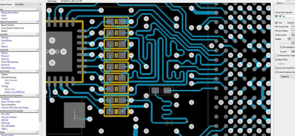
Component Placement
Proper component placement is crucial for optimal PCB performance. It is important to consider the placement of components relative to one another, as well as their placement in relation to the power and ground planes. When placing components, it is important to ensure that there is enough space between them to avoid interference and to allow for proper cooling. Additionally, components should be placed in a way that allows for easy access during assembly and maintenance.
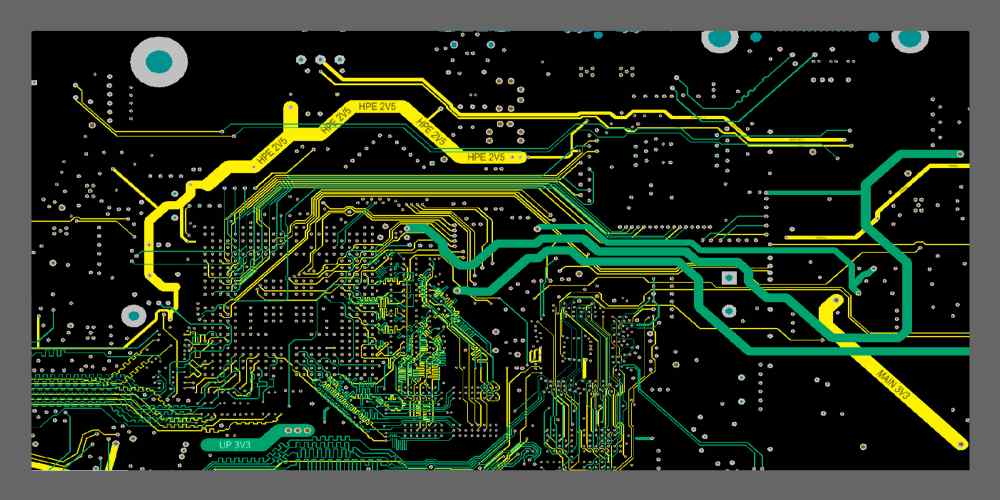
Trace Routing
Trace routing is the process of connecting components on a PCB with conductive traces. When routing traces, it is important to minimize their length and to avoid crossing over one another. This helps to reduce interference and crosstalk. Additionally, traces should be routed in a way that allows for easy access during assembly and maintenance.
Power and Ground Planes
Power and ground planes are critical components of a PCB design. These planes help to provide stable power and ground connections, which are essential for proper circuit operation. When designing power and ground planes, it is important to ensure that they are large enough to handle the required current and that they are properly connected to all components.
Signal Integrity
Signal integrity is the ability of a circuit to transmit signals without distortion or interference. When designing a PCB, it is important to consider the effects of signal degradation and to take steps to minimize it. This can include using proper trace routing techniques, minimizing the length of traces, and using shielding and filtering where necessary.
In summary, when designing an SMD PCB, it is important to consider component placement, trace routing, power and ground planes, and signal integrity. By keeping these considerations in mind, you can help to ensure optimal PCB performance.
Software Tools
When it comes to designing SMD PCB layouts, having the right software tools can make all the difference. There are several options available, but here are three of the most popular:
Eagle
Eagle is a widely-used PCB design software that offers a range of features for both beginners and advanced users. It has a user-friendly interface, and the schematic editor and layout editor are easy to use. Eagle also has a large community of users who share libraries, tutorials, and other resources. However, the free version of Eagle has some limitations, such as a smaller board size limit and a limited number of schematic sheets.
Altium Designer
Altium Designer is a professional-grade PCB design software that offers advanced features and tools. It has a range of features for schematic capture, layout design, and library management. Altium Designer also has a powerful design rule checking system and offers 3D visualization of the PCB layout. However, Altium Designer is expensive and may not be suitable for hobbyists or small projects.
KiCAD
KiCAD is a free and open-source PCB design software that is gaining popularity among hobbyists and professionals alike. It offers a range of features for schematic capture, PCB layout, and 3D visualization. KiCAD also has a large community of users who share libraries, tutorials, and other resources. However, KiCAD has a steeper learning curve compared to other software tools, and some users may find the interface less user-friendly.
In summary, choosing the right software tool for SMD PCB layout design depends on your specific needs and budget. Eagle is a good option for beginners, Altium Designer is ideal for advanced users, and KiCAD is a great free and open-source option.
Manufacturing Process

Solder Paste Application
The first step in the manufacturing process of SMD PCBs is applying the solder paste to the board. This is done using a stencil that is aligned over the board, and then the paste is applied through the stencil onto the board. The stencil ensures that the paste is applied only to the areas where components will be placed.
Pick and Place Machine
Once the solder paste has been applied, the board is moved to the pick and place machine. This machine uses a camera to locate the components and then picks them up and places them onto the board in the correct position. The machine is programmed with the exact locations of each component, and it can place hundreds of components per minute.
Reflow Soldering
After the components have been placed onto the board, the board is moved to the reflow soldering machine. This machine heats the board to a high temperature, causing the solder paste to melt and bond the components to the board. The temperature is carefully controlled to ensure that the solder melts and flows properly, but does not damage the components.
Inspection
The final step in the manufacturing process is inspection. The board is inspected to ensure that all components are in the correct position and that the solder joints are properly formed. Automated optical inspection (AOI) machines are often used for this step, as they can quickly and accurately inspect the board for defects.
Overall, the manufacturing process for SMD PCBs is highly automated and efficient, allowing for large volumes of boards to be produced quickly and accurately.
Testing and Troubleshooting
When designing an SMD PCB layout, testing and troubleshooting are critical steps to ensure that the PCB functions as intended. Testing and troubleshooting should be performed at various stages of the design process, including during the layout phase, after assembly, and before final product delivery.
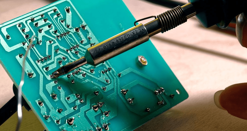
Visual Inspection
Visual inspection is an essential step in testing and troubleshooting an SMD PCB layout. During the inspection, the PCB is examined for any physical damage or defects, such as broken traces, missing components, or solder bridges. A magnifying glass or microscope may be used to inspect the PCB and identify any defects that are difficult to see with the naked eye.
Functional Test
A functional test is performed to ensure that the PCB is operating correctly. This test involves applying power to the PCB and verifying that all components are functioning as intended. The functional test may include measuring voltages and currents, verifying signal integrity, and checking the functionality of any onboard microcontrollers or other programmable devices.
Boundary Scan
Boundary scan is a testing technique that can be used to verify the connectivity of components on an SMD PCB layout. This technique uses a scan chain to test the input and output pins of each component on the PCB. Boundary scan can be used to identify any connectivity issues, such as open circuits or short circuits, and can help to identify the location of the problem.
In conclusion, testing and troubleshooting are critical steps in the SMD PCB layout design process. Visual inspection, functional testing, and boundary scan are all important techniques that can be used to identify and resolve any issues with the PCB. By performing these tests at various stages of the design process, designers can ensure that their SMD PCB layout is functioning correctly and is ready for final product delivery.
Conclusion
In conclusion, SMD PCB layout is an essential aspect of modern electronic design. It offers numerous advantages over traditional through-hole components, including smaller size, greater reliability, and improved performance. By following best practices for SMD layout, designers can ensure that their circuits perform optimally while minimizing potential issues such as noise, crosstalk, and EMI.
Some key takeaways from this article include:
- Always use a ground plane to reduce noise and improve signal integrity.
- Place decoupling capacitors as close to the power pins of each component as possible to minimize voltage fluctuations.
- Use proper spacing and routing techniques to reduce crosstalk and EMI.
- Consider the thermal requirements of your components and design accordingly to prevent overheating.
By following these guidelines and taking care to optimize your SMD PCB layout, you can create circuits that are reliable, efficient, and high-performing. Remember to always test your designs thoroughly and make adjustments as necessary to ensure that they meet your specifications and requirements.
