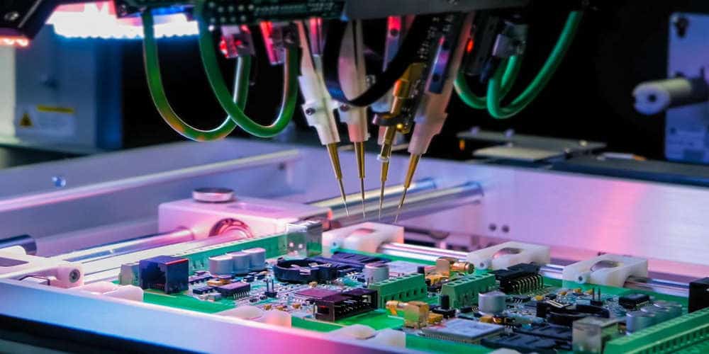
Solid-state drives (SSDs) have become increasingly popular in recent years due to their faster read and write speeds compared to traditional hard disk drives (HDDs). The key to their performance lies in the design of the SSD printed circuit board (PCB). The PCB is responsible for connecting all the components of the SSD and ensuring they work together efficiently.
SSD PCB design is a complex process that requires a great deal of expertise. The design must take into account factors such as signal integrity, power delivery, and thermal management. The layout of the PCB must also be optimized to minimize signal noise and interference.
In this article, we will explore the various aspects of SSD PCB design and how they impact the performance of the drive. We will discuss the key components of an SSD PCB, including the controller, NAND flash memory, and power management circuitry. We will also examine the different design considerations that must be taken into account, such as trace routing, layer stacking, and thermal management. By the end of this article, you will have a better understanding of the importance of SSD PCB design and how it impacts the performance of your storage device.
SSD PCB Design Basics
SSD PCB Design Overview
Solid State Drives (SSDs) are becoming increasingly popular due to their high speed, low power consumption, and high reliability. SSDs use NAND flash memory chips to store data, and the SSD Printed Circuit Board (PCB) connects these chips to the computer’s motherboard.
The SSD PCB design must be carefully crafted to ensure that the SSD operates reliably and efficiently. The PCB design plays a critical role in the performance and reliability of the SSD.
SSD PCB Design Considerations
There are several considerations that must be taken into account when designing an SSD PCB:
-
Signal Integrity: The signals between the NAND flash memory chips and the controller must be carefully designed to ensure that they are transmitted accurately and reliably. High-speed signals require careful attention to routing, termination, and impedance matching.
-
Power Integrity: The power supply to the NAND flash memory chips must be carefully designed to ensure that it is stable and clean. Any noise or instability in the power supply can cause data corruption or loss.
-
Thermal Management: SSDs generate heat during operation, and the PCB must be designed to dissipate this heat effectively. Failure to manage the heat can cause the SSD to overheat, which can lead to data loss or damage to the SSD.
-
Mechanical Design: The mechanical design of the SSD PCB is critical to ensure that it fits into the computer’s housing and interfaces with the motherboard correctly. The PCB must be designed to withstand mechanical stress and vibration.
In conclusion, SSD PCB design is a critical aspect of SSD design. The PCB must be designed to ensure that the SSD operates reliably and efficiently. Signal integrity, power integrity, thermal management, and mechanical design are all essential considerations when designing an SSD PCB.
SSD PCB Design Process

SSD PCB Design Steps
The process of designing an SSD PCB involves several steps that need to be followed in a specific order. Here are the steps involved in SSD PCB design:
-
System Requirement Analysis: The first step is to analyze the system requirements and determine the specifications of the SSD PCB. This includes determining the capacity, performance, and interface requirements.
-
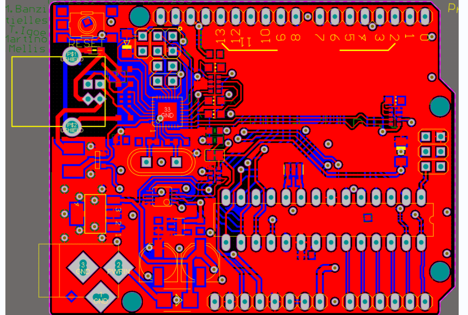
Schematic Design: The next step is to create a schematic design of the SSD PCB. This involves creating a diagram that shows the connections between the various components on the board.
-
PCB Layout Design: Once the schematic design is finalized, the next step is to create a layout design of the PCB. This involves placing the components on the board and routing the connections between them.
-
Design Verification: After the layout design is completed, the next step is to verify the design. This involves checking for errors and ensuring that the design meets the system requirements.
-
Prototype Production: Once the design is verified, the next step is to produce a prototype of the SSD PCB. This involves manufacturing the PCB and assembling the components onto it.
-
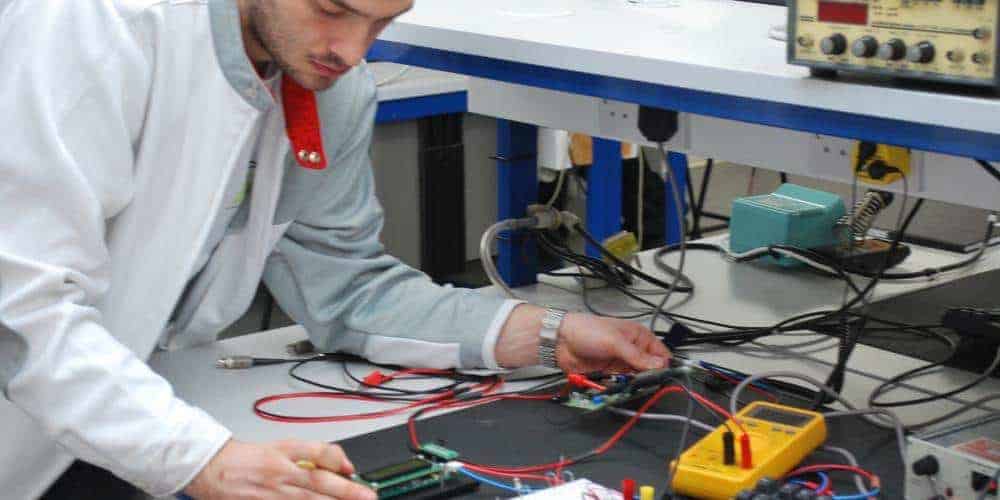
Testing and Validation: The final step is to test and validate the prototype. This involves checking that the SSD PCB meets the system requirements and performs as expected.
SSD PCB Design Tools

There are several tools that can be used for SSD PCB design. Here are some of the most commonly used tools:
-
Schematic Design Tools: These tools are used to create a schematic design of the SSD PCB. Examples include Altium Designer, Eagle PCB, and KiCAD.
-
PCB Layout Design Tools: These tools are used to create a layout design of the PCB. Examples include Altium Designer, Eagle PCB, and KiCAD.
-
Simulation Tools: These tools are used to simulate the behavior of the SSD PCB. Examples include LTSpice and PSpice.
-
Testing Tools: These tools are used to test and validate the SSD PCB. Examples include oscilloscopes, logic analyzers, and function generators.
In conclusion, designing an SSD PCB involves several steps, including system requirement analysis, schematic design, PCB layout design, design verification, prototype production, and testing and validation. There are several tools available for SSD PCB design, including schematic design tools, PCB layout design tools, simulation tools, and testing tools.
SSD PCB Design Best Practices
When designing an SSD PCB, there are several best practices that should be followed to ensure optimal performance and reliability. Here are some of the key considerations to keep in mind:
-
Component Placement: Proper component placement is critical for signal integrity and thermal management. Place high-speed components closer to the controller to minimize signal loss and noise. Also, place power-hungry components away from sensitive circuitry to avoid interference.
-
Trace Routing: Keep trace lengths as short as possible to minimize signal delay and loss. Use wider traces for high-current components to reduce resistance and heat generation. Also, avoid sharp bends and corners in traces to prevent signal reflections and crosstalk.
-
Power Delivery: Ensure that the power delivery network is robust and can handle the peak current demands of the SSD. Use multiple power planes to minimize voltage drop and noise. Also, place decoupling capacitors near power-hungry components to reduce noise and stabilize the power supply.
-
Thermal Management: SSDs generate a lot of heat, so proper thermal management is crucial to prevent overheating and component failure. Use thermal vias to dissipate heat from the components to the ground plane. Also, place thermal pads on high-power components to improve heat transfer to the PCB.
-
Testing and Validation: Test the PCB thoroughly before production to ensure that it meets the performance and reliability requirements. Use simulation tools to verify signal integrity and thermal management. Also, perform environmental and reliability testing to ensure that the SSD can withstand harsh operating conditions.
By following these best practices, designers can create SSD PCBs that are optimized for performance, reliability, and longevity.
SSD PCB Design Challenges
SSD PCB Design Challenges Overview
Solid State Drives (SSDs) have become increasingly popular due to their speed, durability, and reliability. However, designing a Printed Circuit Board (PCB) for an SSD presents unique challenges that must be addressed to ensure the device functions optimally.
One of the primary challenges of SSD PCB design is the need to balance performance, cost, and reliability. SSDs require a complex PCB design that includes multiple layers, high-speed signaling, and power management. These factors can increase the cost of the PCB and make it more challenging to manufacture.
Another challenge is the need to manage heat generated by the SSD. High-performance SSDs generate a significant amount of heat, which can cause reliability issues if not managed correctly. PCB designers must consider various heat management techniques, such as thermal vias, heat sinks, and thermal pads, to ensure the SSD operates within acceptable temperature ranges.
SSD PCB Design Challenges Solutions
To address the challenges of SSD PCB design, several solutions are available. One approach is to use specialized software tools that can simulate the performance of the PCB design and identify potential issues before manufacturing. These tools can help PCB designers optimize the design for performance, cost, and reliability.
Another solution is to use advanced PCB materials that can handle the high-speed signaling and manage heat effectively. For example, using materials such as Rogers 4350B or Isola FR408 can improve the performance and reliability of the SSD.
PCB designers can also use various design techniques to manage heat and optimize the performance of the SSD. For example, adding thermal vias to the PCB can help dissipate heat, while using a multilayer PCB design can reduce signal noise and improve performance.
In conclusion, designing a PCB for an SSD presents unique challenges that must be addressed to ensure optimal performance, cost, and reliability. By using specialized software tools, advanced PCB materials, and design techniques, PCB designers can overcome these challenges and create high-performance, reliable SSDs.
SSD PCB Design Future Trends
As the demand for faster and more reliable storage devices continues to grow, the future of SSD PCB design looks promising. Here are some of the latest trends in SSD PCB design:
-
NVMe: Non-Volatile Memory Express (NVMe) is becoming the standard interface for SSDs. It provides faster data transfer rates and lower latency compared to the older SATA interface.
-
3D NAND: 3D NAND flash memory is becoming more popular in SSDs. It allows for higher storage densities and lower power consumption.
-
PCIe Gen4: The latest PCIe Gen4 interface provides even faster data transfer rates compared to PCIe Gen3. This will allow for even faster SSDs.
-
Custom Controllers: Custom controllers are becoming more common in SSDs. They allow for better optimization of the SSD for specific applications.
-
Increased Capacities: As the cost of flash memory continues to decrease, we can expect to see even higher capacity SSDs in the future.
Overall, the future of SSD PCB design looks very promising. With faster interfaces, higher storage densities, and custom controllers, we can expect to see even faster and more reliable SSDs in the future.
