Printed Circuit Boards have, without a doubt, become a significant part of this technological error. Since we hit this era, gadgets have been growing smaller and smaller each day. We came from CRT Televisions to the flat screens that we use today, from the large antenna phones to the slim smartphones in the market today. All this has become possible partly due to a complex, thin component known as a Printed Circuit Board.
These components help technicians eliminate the overutilization of wires by bringing in copper traces to transfer electric signals. By doing so, manufacturers can produce incredibly slim gadgets without breaking a sweat. However, building the actual PCB tends to be a bit of a hassle for many PCB manufacturers. Therefore, not many tackle this task with great finesse. But what does the Modern Printed Circuit Boards manufacturing process entail? And how does a PCB manufacturing company offer PCB assembly services?
What exactly is the Printed Circuit Boards Production Process?
To ensure they produce functional Printed Circuit Boards, every PCB manufacturing company must utilize some tricks and pass the unfinished PCB through several complex stages. Moreover, even though circuit boards might be multi, double, or single-layered, the manufacturing method that technicians utilize is the same and only starts to differ after the production of the first layer. With this in mind, some Printed Circuit Boards might take twenty or even more stages throughout the manufacturing process due to the changes in the Printed Circuit Board’s construction. As a result, the multilayers will take more time, while the double and single-layer Printed Circuit Boards will take relatively shorter periods.
The board’s complexity is inversely correlated with the number of processes it has to go through to be functional. Moreover, if the technician skips or shortens any PCB manufacturing phases, the results tend to be detrimental to the board’s performance more so if the technician was undertaking a custom PCB manufacturing process. However, if production takes place without any hitches or errors, then the end product should be a functional Printed Circuit Board.
Components of a Printed Circuit Board
Printed Circuit Board pcb have four primary components, namely:
Substrates
The substrate component, typically made out of fiberglass, is basically the most crucial PCB component you will find out there. Manufacturers employ this component because it offers the Printed Circuit Board incredible core strength and helps it resist breakage. Basically, this component acts like the board’s skeleton.
Copper Layer
The copper layer can contain a complete copper covering or a simple copper foil, depending on the kind of PCB you are producing. Moreover, whatever method a technician chooses to apply, the copper’s purpose will always remain a constant:
– To efficiently transmit electric signals to the various components that depend on the printed circuit board. Basically, copper in a PCB acts like a human’s nervous system.
Solder Mask
The solder mask is the third most crucial component of the printed circuit board. Typically, a solder mask is a pretty smooth polymer layer that technicians utilize to help shield the copper traces from external damage. Moreover, this layer also protects the Printed Circuit Board from environment-induced short circuits, which keeps the circuit board functional for longer.
Basically, the solder mask serves as the board’s “skin.”
Silkscreen
Silkscreen is typically the last component you will find on a printed Circuit Board. Technicians utilize this part to write important information on the Printed Circuit Board. You can find crucial information such as:
– The board serial number
– The board’s electronics manufacturing company’s logo
– Details about switch settings
– Component reference
– Test points and so on
Moreover, silkscreen also goes by two more names which are:
– Legend and,
– Nomenclature
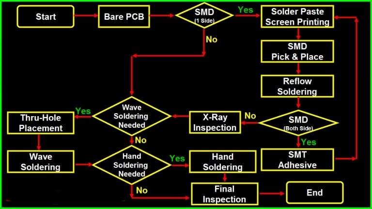
The Printed Circuit Board Manufacturing Procedure
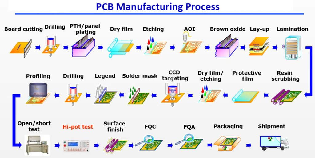
Now that we have the essential components of a Printed Circuit Board out of the way let us go through the printed circuit board production process.
The Printed Circuit Board production process phases start with the design stage and continue to the board’s fabrication. However, to guarantee accuracy and avoid incomplete circuits and short circuits, many of the steps in the PCB manufacturing process are machine-driven and computer guided.
Moreover, before packing the PCB and sending it to the client, technicians must pass the PCB through rigorous testing. Doing so catches any errors before it is too late.
Stage 1: The Designing Phase
The first phase of any printed circuit board manufacturing process is always the designing phase. That is because the PCB manufacturing process must always begin with a plan, and the designing phase offers precisely that, a plan. PCB designers in this phase produce a complex blueprint that contains all the details that the manufacturers require to make a PCB.
To create this complex PCB blueprint, PCB designers rely on PCB designing software programs such as the Extended Gerber Program, which also goes by the name IX274X.
Extended Gerber software efficiently encodes all the info that the PCB designer needs, for example:
– Solder mask information
– Copper layers information
– Other component notations
With this information taken care of, designers can produce professional output format files.
After encoding the PCB’s blueprint using Gerber Extended, the designer then have to check on the design again to ensure that it does not contain any errors.
When this phase is over, the designer can now send the PCB design to the fabrication house for fabrication. Upon arrival, technicians in the PCB fabrication house have to review the design again to confirm that it has no errors. During this review, technicians also verify whether or not the PCB design meets the minimum production tolerance rate. If the PCB design passes this phase, it can move on to the next stage: engineering questions and design review.
Stage 2: Design Review and Engineering Questions
Before producing a printed circuit board, the manufacturer has to ensure that its design does not contain any flaws, which is crucial. Therefore, PCB manufacturers assign engineers a task that involves reviewing the board’s design again to avoid making erroneous PCBs. However, instead of just reviewing the general parts of the PCB, engineers in this stage have to go through all the components of the PCB to ensure that they are all present. Moreover, engineers also have to check on the board’s structure to ensure it is functional.
If the board has no flaws at this stage, the engineer clears it for production.
Stage 3: PCB Printing
When all the design reviews are over, the printed circuit board design is not ready for printing. However, unlike other blueprints, for instance, architectural drawings, technicians can’t print PCB plans on 8.5 x 11 inches paper. Instead, technicians utilize a unique type of printer, which they call a plotter. After receiving PCB designs from the technician, the plotter automatically produces films containing the design. The film is typically the photo-negative version of the PCB design. Therefore technicians can utilize it to carry out production with much ease.
The plotter utilizes two ink versions to bring out the board’s inner layers:
Black ink
The black ink on the film simply represents the board’s circuits and copper traces. It shows the board’s circuit pathway.
Clear ink
Clear ink, on the other hand, represents the parts of the PCB that will be non-conductive, for example, the glass fiber.
As for the board’s outer layers, the plotter simply reverses the entire color sequence. With this in mind, the clear ink tends to represent the copper pathways, while the black ink represents the parts where the copper will be etched. Manufacturers in the pcb industry follow this ink formation each time.
For each printed circuit board layer, manufacturers must also produce an accompanying solder mask. Therefore, for a two-layer printed circuit board, the manufacturer must produce four sheets to carry out production.
When technicians are done printing the films, they then have to line them up and punch a hole through them using a punch-hole machine. The holes they make on these sheets are known as registration holes, and they later utilize them for alignment purposes.
Stage 4: Copper Printing for the Inner Layers
During this phase, the manufacturers start building the Printed Circuit Board.
After printing the circuit board design onto a laminate, technicians at this stage must add a copper coating or a thin copper foil onto the laminate. They then have to pre-bond the copper to the laminate since this laminate acts as the board’s structure. Later, the technicians must etch off the excess copper to reveal the board’s blueprint.
Next, technicians must cover the laminate panel using a photoresist. The resist contains a photoreactive chemical that hardens after UV light exposure. With the resist in place, technicians can efficiently produce a replica of the blueprint on the photoresist.
Using the registration holes from earlier, technicians align the laminate and the resist, then blast them with UV light. When this is done, the ultraviolet light goes through the parts of the film that are translucent, hardening the pre-placed photoresist in the process. The parts that contain the photoresist are, of course, the areas that will make up the board’s copper pathway. Once this process is complete, technicians have to clean the board using a solution that is alkaline. The alkaline solution instantly removes any excess photoresist. However, to ensure that the board is clean, technicians must pressure wash it to remove any dirt on its surface. They then leave the board to dry before moving on to the next phase.
However, before proceeding, technicians must review the PCB to ensure that it does not have any errors until this stage. If the technicians don’t find any errors on the board, they can proceed to the next phase.
Stage 5: Etching
To produce a functional circuit board, technicians must remove the excess copper particle on the board’s inner layers or core. For them to accomplish this task, they must carry out etching. Etching involves covering all the necessary Cu on the circuit board and leaving the rest bare. The technicians then expose the bare circuit board copper particles to a chemical that “eat” them away.
The board can move on to the next phase when the etching is complete.
For multilayer Printed Circuit Board
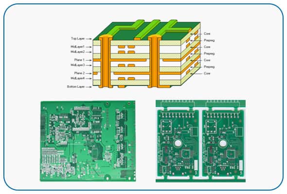
If a manufacturer is producing a Multilayer Printed Circuit Board, they have to pass their unfinished PCB through some extra steps. These additional steps are as follows:
Inner Layer Imaging
The inner layer imaging process is similar to the print process. First, technicians print the design using a printer. They then print a corresponding solder mask film. After aligning these two components, they punch out a registration hole that they utilize to align the two later.
When this process is complete, technicians then:
– Laminate the inner layer
– Align the two-layer using the pre-made registration holes
– Expose the films to UV light while covering the crucial parts with a resist
Etching the Inner Layer
The etching process for multilayer PCBs is similar to that of single and double-layer PCBs. Technicians bathe the PCB using a chemical solvent while covering the copper pathways. The exposed copper parts are eaten away by the chemical.
Resist Stripping
Resist stripping, as the name indicates, involves removing extra resist on the multilayer Printed Circuit Board. The board can move on to the next part when this step is complete.
Post Etch Punching
During post-etching, technicians align all printed circuit board layers using the pre-made registration holes. After aligning them, they punch a precise measure hole through all the layers. The process, however, does not occur manually. Instead, technicians have to utilize a computer to achieve precision.
When this process is complete, the printed circuit board moves on to the auto-optical inner layer inspection.
Inner Layer Inspection
In this phase, the technician utilizes a computer to perform the auto-optical inspection on the inner PCB layers. The auto inspection computer check for:
– Incomplete patterns
– And excess resist
If the PCB has no flaws at this stage, it can move on to the next phase.
Inner Layer Oxide
To enhance the bonding capabilities of the insulating epoxy resin and the copper foil layer, technicians apply an oxide on the inner layers of the PCB.
Lay-up
The layering up process occurs when technicians utilize a unique machine to line up the PCB layers accurately, heat them up, and then bond them with:
– An insulating component between the outer and the inner layer
– And a layer of copper foil
To ensure accuracy, technicians also utilize a computer for this process.
Lamination
For lamination, technicians utilize heat and pressure to efficiently bond the epoxy layers. If a Printed Circuit Board is properly laminated, it tends to hold its layers together more efficiently and with excellent insulation in between the layer.
Ex-Ray Alignment
During the drilling process of a multilayer printed circuit board, technicians utilize an X-ray to ensure perfect alignment of the drilling bit. The vias that the technicians make during this process help electrical engineers quickly secure various components onto the board after the PCB assembly process. Moreover, the vias also help technicians make different connections between the layers of the multi-layer printed circuit board. Therefore, accuracy is pretty crucial in this case, as any miscalculation could render the printed circuit board useless.
When this alignment is complete, the PCB undergoes vias drilling and then moves on to the next phase.
Stage 6: Layer Alignment (for the single and double-layer Printed Circuit Boards)
Since single and double layer Printed Circuit boards only have a maximum of for layer, including the solder mask, the layer alignment process is pretty simple. Like in the multilayer process, technicians align the printed circuit board layers using the registration holes. They then place the layers on a punch machine which drives pins down the registration holes lining up the layers perfectly.
Stage 7: Automatic Optical Inspection
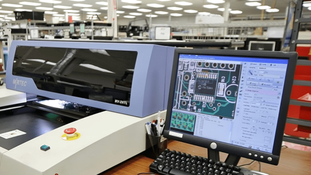
The AOI machine is an automated machine that performs the optical inspection on the printed circuit board. Using this machine, technicians quickly inspect the different layers on a printed circuit board. If the device finds any errors, it reports to the technicians instantly, and the technicians take care of it.
The AOI machine uses the earlier blueprint to inspect the printed circuit board. If it spots any design difference, it automatically flags this as a flaw.
Stage 8: Lamination
After confirming that the Printed Circuit Board layers are defect free, it is time to move on to the lamination phase. The lamination phase, however, occurs in two varying steps:
– The laying up phase
– The lamination step
At this stage, the outer layers of the Printed Circuit Board contain fiberglass that is pre-soaked with a smooth epoxy resin. Moreover, the board’s original substrate contains an extra layer of copper foil that bears the board’s copper traces.
When the outer and inner layers are ready, technicians can now proceed to bond them together.
To sandwich the different layers of PCB, technicians utilize a unique table that contains metal clamps. Technicians position the board on the table using special pins. They then secure them using metal clamps. After this is done, the technician starts to stack various components onto the PCB. These components include:
– A layer of epoxy resin
– A substrate layer
– A copper foil
After aligning the stack perfectly, the technicians then move it to a mechanical press whey they press the stack, binding the different layers together.
Once the binding process is complete, technicians have to eject the board from the press machine, and if everything is good, the board can move on to the next phase.
Stage 9: Drilling
The drilling process of a single and a double-sided PCB is pretty similar to that of a multi-layer PCB. First, technicians utilize an X-ray gadget to align and spot the drilling spots. The drilling machine then drills guiding vias on the PCB layers to secure the stack before drilling the crucial holes. When this is complete, the technician utilizes a computer-aided drill to create multiple vias on the board while referring to the Gerber files.
When drilling is over, the technician removes excess copper and releases the board to move on to the next phase.
Stage 10: PCB Plating
The Printed Circuit Board plating process involves utilizing chemicals to fuse all the layers of the circuit board efficiently. Moreover, the plating chemical also covers the drilled vias on the board, increasing the board’s durability.
Stage 11: Imaging the Outer Layer
Earlier on, technicians applied a resist on the board’s panel. In this phase, technicians must apply another layer of resist, not on the inside layer but the outside layer. The resist protects the PCB during the imaging process. Moreover, after applying resist, technicians carry out imaging on the printed circuit board.
You should note, however, that the outer layer also gets an extra layer of tin which helps shield the outer layer during etching.
Stage 12: Etching the Outer Layer
During this process, technicians keep the printed circuit board on a chemical solvent that removes any unwanted copper particles. In addition, the tin coating protects the necessary copper particles.
When this stage is complete, the PCB is ready for AOI testing.
Stage 13: AOI Testing for the Outer Layer
Just like the inner PCB layers, the outer circuit board layers must also go through an AOI test. Using an auto optical machine, the technicians inspect the outer layer and make sure that it satisfies the requirements on the Gerber File.
Stage 14: Solder Mask Application
After Outer AOI testing, the circuit board is now ready for the application of the solder mask. However, before application, technicians must first clean the PCB. Once clean, the PCB panels each have a solder mask and an epoxy film encasing the surface. Next, UV light strikes the PCB, and it indicates the parts that need solder mask removal.
After removing the excess solder mask, the PCB can then proceed to the oven to efficiently cure the solder mask.

Stage 15: Application of Silkscreen and Surface Finish on the Printed Circuit Board
Since technicians need to imprint crucial information on the PCB, they place a layer known as a silkscreen on the board. They then imprint information that includes:
– Part number
– Manufacturers logo
– Warning label
– Company Identification Number
– Pin locators, et cetera.
When the imprint process is over, technicians apply a surface finish on the board, and now the PCB is complete. However, before they can deliver the board to the client, they have to run a couple of tests which include:
– Electrical reliability test
– Visual inspection
– Quality check
They then have to undertake route out and profiling to ease the shipment process as most PCB companies handle multiple orders from multiple clients. More so, some undertake multiple custom PCB manufacturing processes, hence sorting is crucial.
After this is done, the manufacturers can now deliver the functional printed circuit board to their clients.
Conclusion
The Printed Circuit Board production process can be hectic if you go at it without a clue about what it entails. Moreover, it is procedural, and messing up one stage can cause adverse effects on the final product. However, if you follow the guidelines in this article, you will always produce a functional printed circuit board.
