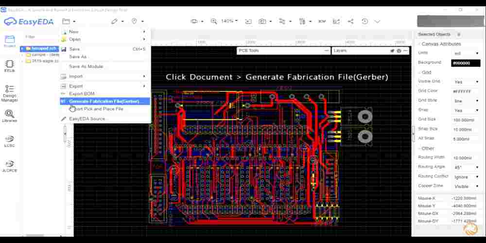
When it comes to designing and manufacturing printed circuit boards (PCBs), the Gerber file output is a crucial step in the process. These files serve as the blueprints for PCB fabrication, containing all the necessary information needed by the manufacturer. As such, it’s essential to pay attention to specific aspects of the Gerber file output to ensure a seamless transition from design to production, and ultimately, a successful end product.
The following discussion highlights nine questions every designer should consider when generating Gerber file output. These questions are aimed at helping you identify potential issues before they become costly mistakes in the production process, maintaining overall quality, and ensuring the final PCBs function as intended.
By addressing factors such as layer stack-up, drill hole information, and file format compatibility, you can take a proactive approach to optimize your Gerber file output. This can result in reduced turnaround times, increased cost efficiency, and enhanced product performance. So, let’s dive into the critical elements you need to pay attention to as you create your Gerber files.
Understanding Gerber Files
Gerber files are a standard file format used in the printed circuit board (PCB) industry for conveying design information to manufacturing equipment. These files contain essential data for PCB fabrication, including layer information, copper traces, drill holes, and component placement. Understanding Gerber files can help ensure a smooth manufacturing process and high-quality end product.
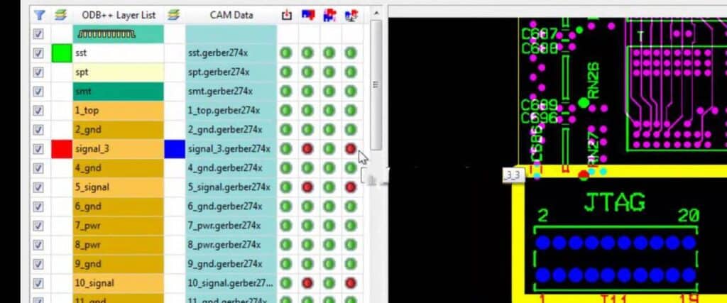
When working with Gerber files, it is crucial to understand the different elements that compose a complete set of files for a PCB design. Typically, a Gerber file set includes:
- Top and bottom copper layers: These files indicate the copper traces’ layout, pads, and vias on the PCB’s top and bottom sides.
- Solder mask layers: These files define the areas where the solder mask should be applied to prevent solder bridges between adjacent traces and pads.
- Silk screen layers: These files contain designators, symbols, and text printed on the PCB, which aid in assembly and debugging.
- Drill file: This file provides the coordinates and sizes of all the holes needed to be drilled on the PCB.
When creating Gerber files for output, it is essential to keep in mind the following questions:
- Are the file units (inches or millimeters) correctly specified and consistent across all layers?
- Are the coordinate format and precision consistent with the manufacturing equipment requirements?
- Have all design rule checks (DRC) been performed to verify the design’s manufacturability?
- Are the layer orientations and stack-up properly defined?
- Have any “unused” copper areas been removed or isolated from the rest of the copper layout?
- Are the reference designators and other text elements legible and correctly placed?
- Has the drill file been generated in the appropriate format, such as Excellon or Gerber X2?
- Are the board outline and any internal cutouts accurately depicted and included?
- Have all the files necessary for the specific PCB fabrication process been included in the output package?
Paying close attention to these questions when outputting Gerber files can significantly reduce the risk of errors and delays in the manufacturing process.
Key Elements in Gerber Files Output
Gerber files are an essential part of the Printed Circuit Board (PCB) design and manufacturing process, as they provide the necessary data for producing accurate and reliable PCBs. This section will focus on three key elements in Gerber files output, and highlight the crucial aspects to consider when handling these files.
Layers and Layer Stacks
Layers and layer stacks play a vital role in Gerber files, as they determine the structure, electrical connections, and functionality of the PCB. It’s essential to:
- Use the correct layer types, such as copper, solder mask, and silkscreen, to accurately represent the final PCB design.
- Ensure that layer stack order stays consistent throughout the design and manufacturing process.
- Use proper naming conventions for easy identification of the layers.
Apertures and Pads
Apertures are openings in the phototool, allowing UV light to pass through and exposing the resist layer, defining the features on each layer of the PCB. Pads are used to create connections to components. When working with Gerber files, it’s essential to:
- Check the aperture list for all the shapes and sizes used throughout the design.
- Verify the pad clearance settings to prevent short-circuits or soldering issues.
- Ensure that pad locations match the corresponding component layout.
Drill Information
Drill information is critical to Gerber files output, as it contains the locations and sizes of holes that need to be drilled in the PCB. In this regard, it’s essential to:
- Differentiate between plated and non-plated holes to guarantee proper PCB connectivity.
- Match the size and location of drill holes to the corresponding pads and vias.
- Export drill files separately and make sure they align with the Gerber files.
By paying close attention to these key elements in Gerber files output, designers and manufacturers can work together to create accurate and reliable PCBs, avoiding potential issues in the manufacturing process.
How to Ensure Accurate Gerber File Output

Design Rule Checks
Before generating a Gerber file, it’s essential to perform design rule checks (DRC) to identify any potential errors or discrepancies in your PCB layout. This step helps in catching issues early in the design process, preventing costly and time-consuming revisions later on.
- Run DRC with your PCB design software
- Address any errors or warnings reported
- Double-check critical dimensions and clearances
Confirming Units and Format
To avoid scaling and compatibility issues, always confirm the units (imperial or metric) and coordinate format (absolute or relative) used in your design before exporting the Gerber file:
- Ensure your layout software and the fabrication facility use the same units and format
- Double-check the settings in your PCB layout before exporting
Selecting Proper Gerber File Format
Picking the appropriate Gerber file format for your project is crucial for successful PCB manufacturing. Usually, there are two formats to choose from: RS-274X (Extended Gerber) and RS-274D (Standard Gerber).
- Use RS-274X whenever possible since it includes embedded aperture information
- Opt for RS-274D only if your manufacturer specifically requests it
- Ensure all required layers are included in your output
- Verify the generated files before sending them to the PCB manufacturer
By following the steps outlined in these sub-sections, you can ensure accurate Gerber file output and reduce the likelihood of errors during the PCB manufacturing process.
Common Issues to Be Aware Of
When generating Gerber files, it is essential to pay close attention to several common issues that can arise during the output process. These issues can lead to production errors or delays in manufacturing. Here, we discuss two common issues: Missing or Misaligned Components and Incorrect Drill Sizes.
Missing or Misaligned Components
One common problem encountered when working with Gerber files is missing or misaligned components. This issue can arise due to:
- Errors in the component library
- Incorrect component placement in the design
- Incomplete or inaccurate solder masks
To prevent these issues, follow these tips:
- Ensure that your component libraries are up-to-date and accurate.
- Double-check component placements during design, and consider using the Design Rule Check (DRC) tool to find errors.
- Verify that solder masks are accurately generated and aligned with components.
Incorrect Drill Sizes
Another potential problem when generating Gerber files is the use of incorrect drill sizes. This can lead to:
- Holes that are too small or large for components
- Holes that are the wrong shape
- Difficulty in assembly and potential component damage
To avoid incorrect drill sizes, consider these recommendations:
- Cross-check your design against component datasheets to confirm hole sizes and shapes.
- Verify that your PCB design software is using the correct drill sizes.
- Perform a thorough Design for Manufacturability (DFM) check to catch any potential issues before Gerber file generation.
Final Review and Submission Process
Software Compatibility
Before submitting your Gerber files, ensure that they are compatible with your manufacturer’s software. You can achieve this by:
- Verifying the supported file formats by your manufacturer
- Utilizing a Gerber viewer to preview and confirm the layout
This approach helps to prevent any file-related issues during the manufacturing process.
Sign-off
Upon ensuring software compatibility, it’s crucial to sign off on the design. The sign-off process typically includes:
- Reviewing the details of the design, such as dimensions, traces, and vias
- Checking for any final adjustments that need to be made
- Confirming the functionality and design intent
By verifying every aspect of your design, you can confidently submit it to the manufacturer, minimizing the possibility of any errors or oversights.
Communication with Manufacturers
Maintaining clear communication with your manufacturer is an essential part of the submission process. Keep the following points in mind:
- Provide comprehensive documentation, including specifications, assembly drawings, and bill of materials (BOM)
- Address any special requirements or instructions, including surface finishes or material preferences
- Establish open channels for updates, production feedback, and progress reports
By implementing these practices, you can help facilitate a smooth and efficient production process for your Gerber files.
