Kicad is an excellent free PCB designing package that includes a schematic editor and PCB design tools. It’s a skill that’s definitely worth the time and work it takes to develop. In today’s society, it’s impossible to picture life without technology and, by extension, computer programs.
Many people neglect the significance of electronics as a discipline since everyone focuses on computer and code programming. Therefore, you need an electronic component to implement any computer code.
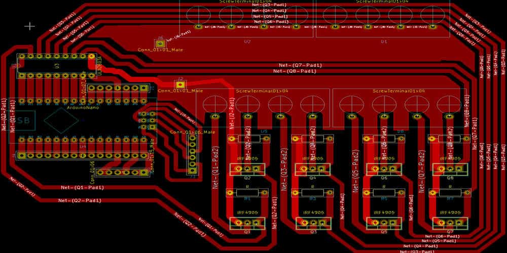
Printed Circuit Boards
If you’ve always been fascinated by electronics and circuitry. You likely picked up on their significance at a young age. While there are several subfields within electronics, testing, assembling, and construction are all crucial. As a result, PCBs are an essential element of electronics that decide whether or not a given device will work.
In the past, circuit boards required continuous end-to-end board wiring. It requires frequent solder to repair the wires. Yet, the prototype’s susceptibility to short-circuiting was discovered after its wire insulations deteriorated and the wires touched one another. There had to be compromise, and the development of PCBs was a huge step forward.
When people talk about “PCBs,” they’re referring to the PCBs that provides electrical and mechanical support for and connect electrical parts. This is possible by etching pads, paths, and other characteristics onto the non-conducting substrate.
So now you know what a printed circuit board is. It’s time to learn about the various parts of a board before diving into Kicad PCB design. If you’re interested in learning more about what goes into making a PCB. We invite you to take a look at the relevant section of our page.
What does a Kicad printed circuit board actually look like? What’s the procedure for making one?
Kicad PCB Design
The term “Kicad PCB” refers to a printed circuit board designed using the Kicad program. There are a number of PCB design software options available, including the commercially available EAGLE; however, Kicad stands out as a particularly strong alternative because of its combination of high productivity and zero cost to the user. Both professionals and beginners make use of this software frequently. The software is compatible with a wide variety of platforms.
What can Kicad PCB Design do?
KiCad is a free and cross-platform program for creating PCBs. And it is also compatible with Mac, Windows, and Linux. Prototypes, students, and engineers all utilize and contribute to KiCAD. Because of its popularity among developers. KiCad is a program used for designing electronic circuits and embedded systems using a graphical user interface. It comes with a wide variety of elements to help you get started right away, such as ICs, resistors of varying values, and LEDs of various colors. Make your schematics and circuit designs in an interactive environment. Then generate Gerber files to get read by Kicad.
KiCAD’s strength is in its adaptability. It’s wonderful for newbies, yet it also contains features that advanced engineers will find useful.
The program offers:
- Support for making PCBs and schematics in-built.
- Router with user input.
- Possibility of incorporating your own 3D elements.
- Software that displays your PCBs in stunning, full 3D.
- Many distinct layout techniques, including some highly efficient grid-aware options for optimizing your board’s footprint. It is crucial while working with limited space.
- Dual-sided and single-sided board support.
- Excellent, and Gerber drill files are just two of the many PCB fabrication formats you may export to.
- Comprehensive help for PCBs with multiple layers.
- Quick to learn and use with no learning curve. The program also has a command-line interface.
- Thorough and upgradable documentation.
- Homebrew and enthusiast-friendly software.
- The open-source KiCad community is always working to refine and enhance the program. Because of its current state of development, you can participate as well.
Creating Kicad PCB Board Outline

We advise using KiCad if you are new to electronics and wish to design your own PCB. Besides being completely free, learning to use KiCad is simple. It’s available for quick and easy installation on macOS or Windows from the main website (no registration required):
Drawing schematics and layout printed circuit board
- The Kicad program can be downloaded from the following link http://kicad-pcb.org/download/ and installed on your computer.
- Initiate a brand-new project right away. Here, launch Kicad and select either the “open” or “create new” option for a project. To start a brand-new project, click “create new” and then select a location on your computer. After that, you can use Eeschema to design your circuit board schematic and layout. The next step is to launch the schematics PCB editor and apply the default configuration.
- To assemble, add parts. The circuit prototypes get depicted on the schematic, which you must draw. Put in all the necessary parts before you start adding wires to show how they’ll get connected. Choose the “place symbol” when adding a part. It will trigger the appearance of the component selector, from where you can select an appropriate match for the element you need, such as a resistor. The next step is to put this symbol into the schematic’s empty slot.
- To connect, wires are required. After you’ve installed everything that needs to get installed, you’ll have to start incorporating the cables. In this case, sketching wires to connect the necessary parts is all that’s required. The “place wire” button on your toolbar will do the trick. Don’t worry if you make a mistake; using the escape key will undo everything you’ve done so far.
- Include numerical values for symbols. Assigning symbolic values to the vast majority of components is now necessary. A battery part, for instance, needs to have a voltage symbol associated with it. So too, a resistor should get represented by the symbol of resistance. Once more, it’s important to remember that changing the values you provide individual components won’t alter the circuit’s behavior.
- Describe the schematic with notes. For this, you’ll need to provide each constituent its own distinct identifier. To give just one example, a resistor may get labeled as R1, R2, R3, and so on if there are two or more of them. The “annotate schematics” option in the menu bar will do the trick.
- Please include schematic symbol footprint filter. In order to go on to the board design phase, you must first create footprints for the elements in your schematic. Important footprints are printable on the PCB board beneath each component. A through-hole resistor, for example, requires two such holes. Simply choose “assign footprint” from the menu of available tools. Kicad has a large library of footprints that may get used. But the filter feature makes finding the right one easy.
- Do an electrical rule checking, often known as the ERC. It’s easy to make a mistake when using Kicad to design PCBs, but mistakes are possible for everyone. Ignoring connecting a component is one example of the kinds of mistakes that must get checked for and fixed. You should run the ERC to find all these problems in your circuit and fix them before moving on. Select ERC in the “inspect” menu and hit “run” to complete the task. In this way, you can see each error as it occurs and fix it as you see fit.
Draw Layout Of The Circuit Board
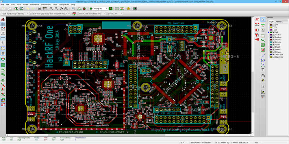
- Create a completely new board design. Transferring the components from the schematic to the board is the next step after specifying their connections there. The first step in creating a board layout is to select “run PCB new to the layout PCB” from the schematic menu. Choose the “open PCB editor” choice from the tool menu to accomplish the same thing.
When you select “update PCB from schematic,” a new window will open where you can get the schematic’s footprints and connections. After the PCB is updated, the loaded footprints will be available, revealing any air wires.
- Get the components in their proper place. Components can get connected by air wires if they get positioned properly. To make the PCB easier, try to avoid having any air wires cross one another. Pressing the “M” key while hovering over a component will cause it to get moved.
- Create the tracks. Once you’re happy with where everything goes, you may replace the air wires with tracking lines to make the connections. When the printed circuit board is finished, all the patterns you drew will be actual top copper layer traces. To create the tracks, select the “route track” option. You may also choose which side of the board you wish to draw on by using the layers manager to switch to the appropriate layer.
- Sketch up the basic shape of your printed circuit board. To complete this step, simply create a polygon and place it on the “edge cuts” layer. After that, you can start sketching by clicking once in each corner. The polygon can get completed by clicking back to its origin.
- Start the design rule validation process. Using the DRC to check for and highlight faults becomes essential. Short widths or the absence of a track are examples of possible mistakes. In addition, the summary includes all the errors that occurred. These may get seen by clicking on the tabs labeled “unconnected things” and “issues.” Afterward, you’ll get prompted to rectify whatever was flagged before moving on.
After finishing the design of your PCB, you can move on to fabricating the actual board. Here, a PCB fabrication business like RayMing Assembly & PCB can be of assistance in getting the board ready for use. Finally, you’ll need to send your Kicad board design files to the appropriate company. In contrast, if you have any queries or concerns concerning the Kicad printed board design files that RayMing uses for production, you may visit their website and get in touch with them there. Once you’ve figured out the specifics, you may input your files via the website and wait for the final outcome.
Draw Electronic Schematics Diagram
1. Launch KiCAD on your computer and go to the main window for the KiCAD project manager. Its associated file type is *.pro. You can now pick from a total of eight different possibilities.
1a. Schematic diagrams are drawn using “Eeschema.” *.sch is the file extension.
1b. Using the “Schematic Library Editor,” you can design and implement components that aren’t found in existing libraries. To be exact, the *.lib extension indicates a library file.
1c. PCBNew initiates the generation of a fresh PCB file. *. kicad_pcb is the file extension for Kicad PCB designs.
1d. PCB Footprint Editor is used to pick THT and SMT component footprints. *.net is the file extension.
1e. Use “GerbView” to make Gerber files.
1f. The bitmap picture gets fed into “Bitmap2Component,” which produces an element and its footprint. The Format of the File Is: *. kicad_mod
1g. PCB Calculator is a tool used to measure and compute various units and dimensions, such as track width, for printed circuit boards.
One h. The purpose of the PL Editor is to alter the parameters of the Page Layout. Kicad-WKs File Format: *. kicad_wks
2. At this point, we’ll officially launch the new endeavor. Choose File > New Project.
Identify the venture by naming it. Create a new file with the “.pro” extension. To store your files, KiCAD will prompt you to make a new folder. To continue, please confirm by clicking yes.

3. We will now proceed to sketch out some sort of diagram. Just hit the link below. Eeschema is the first button on the left.
4. Select the Page Settings menu item now. Schematic titles and other page-setting criteria can get adjusted with this button. Finally, select OK to save the new settings, and you’ll see them appear in the lower-right corner of the schematics. Stop right now and store the schematic layout file. File>> Schematic Project
5. To add a new component to the schematic, click here. This option can get found on the toolbar to the right.
6. A pick component window will open up in the middle of your schematic if you click there. Our next step is to install a resistor. By pressing the R key, you can access the resistor R in the device menu. Choose it, then hit the “OK” button. Now, you can decide where on the page the part will go.
7. You may zoom out and in by using the mouse wheel. Use the middle mouse button to pan in any direction.
8. In contrast to other programs, all you have to do to remove a component is to select it with your mouse and click the “r” key on your computer. This part will move. No action on your part is necessarily required.
9. After the installation of the component, we may modify its parameters by right-clicking it, at which point a menu with various settings will display (as depicted in the following image). You can change the component’s value by hovering over it and pressing the v button.
10. Hovering over the element and pressing delete removes it. When you right-click on it, choose “Delete component” to get rid of it.
11. Click and hold the c key while hovering over the component you want to copy. Now, select the location on the page where you’d like to drop the sheet by clicking on it.
12. Simply right-click the element and choose “Drag component” to move it. Left-click wherever you’d like on this sheet to start dragging.
13. With a right-click on the component, you may access the “Grid choose” menu and modify the snap grid as needed. For schematics, it’s suggested that you use a grid size of 50 mils.
14. Checking for mistakes in the schematics is next. To achieve this, we use Electrical Rule Check. Follow the prompts to run the program by clicking the Run button. Any problems or cautions will get detailed in a report. No warnings or errors are allowable. In the event of a mistake, the schematics will feature a little green arrow pointing to the offending area.
15. The Bill of Materials is made at the end of the process. Eeschema’s Bill of Materials is accessible through the main menu. Upload a plugin (*.xsl, for example) and then press the “Generate” button. This document can get found in the root directory of our project. Open the file in Excel, import the data, and then click the “ok” button.
Designing Tools of KiCad Suite
There are numerous design tools available in the KiCad Suite. The efficiency of this program is due to these tools.
1. Symbol Editor
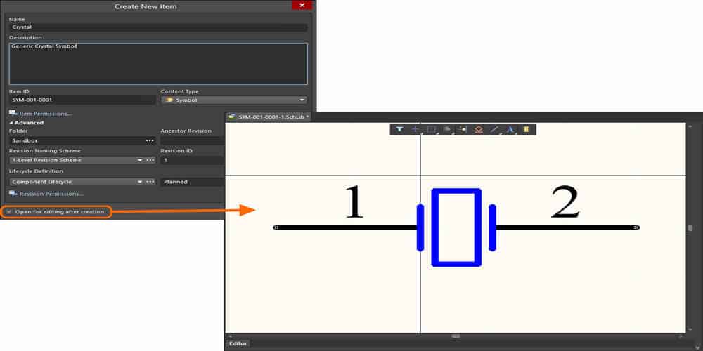
Electronic parts and their connections are graphically depicted in a schematic. New layout symbols that aren’t already available can also get created by using a symbol editor. If you are creating a new IC symbol, for example, you can define its pinout and attributes. You can add this symbol to an existing library or create a new one.
2. Image converter
Incorporating unique logos onto your electronic board that isn’t already in the libraries is simple with the help of the image converter. KiCad has a limited application for working with vector files. This means that raster images can get imported without any prior conversion. In this case, you should use the Image converter. In addition, you may use this function to transform images saved in PNG or JPG format into KiCad-compatible graphics.
3. Gerber viewer
Gerber files include the information required for PCB manufacture. The kicad PCB editor is another useful tool for making these schematics. Once the data gets generated, only a Gerber viewer will be able to open the Gerber files. Having this will allow you to double-check the files before sending them off for manufacturing.
4. Schematic layout editor
A circuit or schematic diagram can get drawn with the use of the schematic editor.
5. Footprint editor
A new footprint can get designed from scratch, or existing ones can be modified with the printed board footprint editor. All of the footprint libraries are also open for customization.
6. Schematic library editor
In a similar manner to the schematic editor is the library editor. Component symbols for use in schematics can get created and managed with the use of the editor for the schematic library.
Keyboard Shortcuts in KiCaD
KiCad supports a variety of shortcut keys. Your work will go more quickly and easily if you know these keypad shortcuts. Furthermore, most of KiCad’s features are accessible using shortcut keys. Here, you’ll learn the most useful and widely used keyboard shortcuts for KiCAD.
· Select an item’s settings with the E key.
· To select and drag an item with the mouse wheel, press the letter M.
· With the G key, you can drag items without severing any connections.
· Press the letter W to select the Wire tool. Connecting parts is made easier with the wire tool.
· The R key allows you to move any object.
· If you are currently looking at a component and want to read its datasheet, press the letter D.
· You may make a duplicate of anything you’re hovering over by pressing the letter C, and the letter X will mirror it along the X-axis.
· To flip an object in the PCB editor, press the letter F.
· To quickly toggle between the printed board editor and the regular editor, use Shift + S on your keyboard. You can get more done in less time with this key.
You should feel comfortable using these shortcuts in your KiCad projects. Furthermore, the Hotkeys part of the settings menu allows you to set your own shortcuts.
FAQs
What is the Footprint Assignment Tool?
Developing a PCB layout follows the completion of a schematic sketch. All sizes and specifications are significant in the PCB layout. Physical or mechanical limitations get imposed on PCB editors. Including footprints with schematic symbols facilitates their transfer to a PCB layout. The footprint assigner has features like the design sign footprint filter i.
In addition, footprints are two-dimensional physical schematics for soldering the real component. To accommodate a five-millimeter LED, for example, the circuit must have footprints with two holes and two pads.
When you launch a footprint assignment tool, a new window will pop up, and it will have three columns. Additionally, footprint sets can be seen in the first column. Several unique traces can be found in a library. It is critical that we identify a footprint and correlate it with schematic symbols.
What is the process for updating a circuit board from a design?
Any changes made in the PCB editor can get transferred to the schematics editor. Select Tools, then update the layout from PCB. The footprint assignment, for example, is changeable. In addition, by synchronizing these updates to the schematic, consistency gets preserved.
Conclusion
With KiCad, you can make all the necessary files for PCB design. Among these are drill files, Gerber files, and component position files used by photoplotters. Electronic hardware development is another area where the KiCad tutorial comes in handy. We hope that this KiCad guide has helped you understand the ins and outs of using this program.
