Designing electronic circuit boards is a complex process that requires careful planning and execution. Electronic circuit boards are used in a wide range of applications, including computers, mobile phones, medical devices, and automotive systems. The design process involves creating a schematic diagram of the circuit, selecting the appropriate components, and laying out the board to ensure proper functionality.
The first step in designing an electronic circuit board is to create a schematic diagram of the circuit. This involves identifying the various components that will be used in the circuit and determining how they will be connected. Once the schematic is complete, the designer can begin selecting the appropriate components for the circuit. This includes choosing the right resistors, capacitors, and other components to ensure that the circuit functions correctly.
Once the components have been selected, the designer can begin laying out the board. This involves determining where each component will be placed on the board and how they will be connected. The layout must be carefully planned to ensure that the board is compact, efficient, and easy to manufacture. By following these steps, designers can create high-quality electronic circuit boards that meet the needs of their clients and customers.
Basics of Electronic Circuit Board Design
Electronic circuit board design is the process of creating a schematic diagram of an electronic circuit and then designing a printed circuit board (PCB) to implement that circuit. Here are some basics of electronic circuit board design:
Schematic Diagram
The first step in designing an electronic circuit board is to create a schematic diagram of the circuit. A schematic diagram is a graphical representation of the circuit that shows how the components are connected. It is important to create a clear and accurate schematic diagram because it will serve as the basis for the PCB design.
PCB Design
The next step in electronic circuit board design is to create the PCB layout. The PCB layout is a detailed design of the physical circuit board that shows the placement of all the components and the routing of the electrical connections. The PCB layout must be designed to ensure that all the components are properly connected and that the board meets the required specifications.
Component Selection
Selecting the right components is an important part of electronic circuit board design. The components must be selected based on their specifications, such as voltage, current, and frequency, and their compatibility with other components in the circuit. It is also important to consider the availability and cost of the components.
Design Rules
Design rules are a set of guidelines that must be followed when designing an electronic circuit board. These rules specify the minimum clearance between components, the minimum trace width, and other important parameters. Following these rules is important to ensure that the board can be manufactured correctly and that it will function properly.
PCB Manufacturing
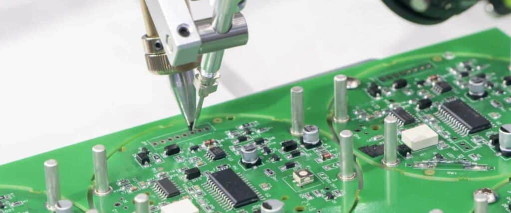
Once the PCB layout is complete, the board can be manufactured. PCB manufacturing involves several steps, including printing the circuit pattern onto the board, drilling holes for the components, and applying a layer of solder mask. The finished board can then be populated with components and tested to ensure that it functions correctly.
In conclusion, electronic circuit board design is a complex process that requires careful planning, attention to detail, and knowledge of electronic components and design principles. By following the basics of electronic circuit board design, you can create a functional and reliable circuit board that meets your requirements.
Tools and Software for Designing Electronic Circuit Boards

Designing electronic circuit boards requires specialized tools and software. Here are some of the most commonly used ones:
Schematic Capture Tools
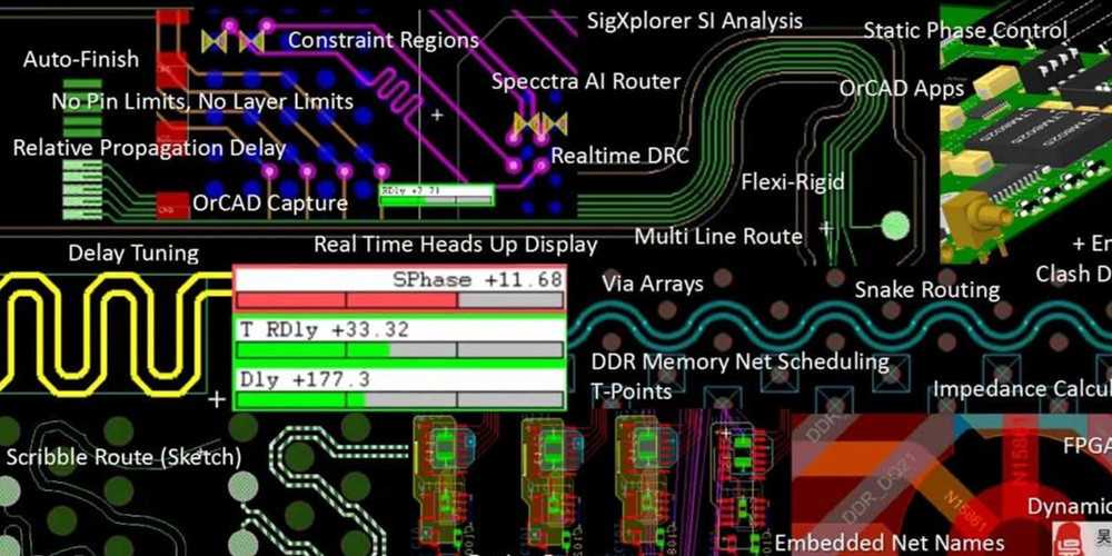
Schematic capture tools are used to create the circuit diagram of the electronic circuit board. Some popular schematic capture tools include Altium Designer, Eagle PCB, and KiCAD.
PCB Layout Tools
PCB layout tools are used to design the physical layout of the electronic circuit board. These tools allow designers to place components, route traces, and perform design rule checks. Some popular PCB layout tools include Altium Designer, Eagle PCB, and KiCAD.
Simulation Tools
Simulation tools are used to simulate the behavior of the electronic circuit board before it is actually built. This can help identify potential design issues and ensure that the circuit works as intended. Some popular simulation tools include LTSpice, PSpice, and CircuitMaker.
PCB Fabrication Tools
PCB fabrication tools are used to create the physical circuit board from the design files. These tools include software for generating Gerber files, which are used by PCB manufacturers to create the board. Some popular PCB fabrication tools include Gerber Viewer, PCB Artist, and EasyEDA.
In addition to these tools, designers may also use oscilloscopes, multimeters, and other test equipment to verify the functionality of their electronic circuit boards.
Design Considerations for Electronic Circuit Boards
When designing electronic circuit boards, there are several factors that must be taken into consideration to ensure that the circuit functions correctly and reliably. Here are some important design considerations to keep in mind:
Component Placement
The placement of components on the circuit board is critical for proper functionality. Components should be placed in a logical and organized manner to minimize the length of the traces that connect them. This reduces the chances of signal interference and crosstalk between components.
Trace Routing
Trace routing is the process of connecting the components on the circuit board with traces. The width and spacing of these traces must be carefully chosen to ensure that they can handle the required current and voltage without overheating or causing interference. Additionally, the traces should be routed in a way that minimizes the length and number of vias, which can introduce signal noise.
Power and Ground Planes
Power and ground planes are large copper areas on the circuit board that provide a low-impedance path for current flow. These planes help to reduce noise and provide a stable voltage reference for the components. When designing the circuit board, it’s important to ensure that the power and ground planes are placed close to each other and that they are connected with multiple vias to minimize the impedance.
Thermal Management
Electronic components generate heat, and if not properly managed, this heat can cause the components to fail prematurely. To prevent this, the circuit board should be designed with proper thermal management in mind. This can include adding thermal vias, using heat sinks, and ensuring that components are properly spaced to allow for adequate airflow.
Overall, designing an electronic circuit board requires careful consideration of many factors. By keeping these design considerations in mind, you can create a circuit board that functions reliably and efficiently.
Testing and Troubleshooting Electronic Circuit Boards
Once the electronic circuit board has been assembled, it is important to test it thoroughly to ensure that it is functioning correctly. Testing and troubleshooting are critical steps in the design process, as they help to identify any errors or issues that may be present in the circuit board.
There are a number of different tools and techniques that can be used to test and troubleshoot electronic circuit boards. Some of the most common methods include:
-
Visual Inspection: This involves examining the circuit board for any physical defects or issues, such as loose connections, damaged components, or incorrect wiring.
-
Functional Testing: This involves testing the circuit board to ensure that it is performing its intended function correctly. This can be done using a variety of tools, such as oscilloscopes, multimeters, and logic analyzers.
-
Boundary Scan Testing: This is a specialized testing technique that is used to test the connections between different components on the circuit board. It involves using a dedicated testing tool called a boundary scan tester.
-
In-Circuit Testing: This involves testing the circuit board while it is still connected to the rest of the system. This can be done using specialized testing equipment, such as in-circuit testers or bed-of-nails testers.
When troubleshooting electronic circuit boards, it is important to approach the problem systematically. This involves breaking the circuit board down into smaller sections and testing each section individually. By doing this, it is possible to isolate the problem and identify the root cause of the issue.
In conclusion, testing and troubleshooting are critical steps in the design process of electronic circuit boards. By using the right tools and techniques, it is possible to identify and resolve any issues that may be present in the circuit board, ensuring that it functions correctly and reliably.
Advanced Techniques for Electronic Circuit Board Design

Designing electronic circuit boards requires a solid understanding of the underlying principles of electronics and a proficiency in using specialized software. To create more complex and sophisticated circuits, advanced techniques are necessary. Here are a few techniques that can be used to design high-quality electronic circuit boards:
-
Multi-layer PCB design: Multi-layer PCBs provide more flexibility in routing the circuit traces, reducing the need for jumpers or vias. They also allow for more compact designs, reducing the overall size of the board. However, the complexity of multi-layer PCBs requires careful planning and attention to detail.
-
High-speed design: High-speed circuits require careful consideration of signal integrity, noise reduction, and impedance matching. Advanced techniques such as differential signaling, controlled impedance routing, and signal termination can help improve the performance of high-speed circuits.
-
Thermal management: Electronic components generate heat, which can affect their performance and lifespan. Advanced thermal management techniques such as heat sinks, thermal vias, and copper pours can help dissipate heat and improve the reliability of the circuit.
-
Design for manufacturing: Designing a circuit board that is easy to manufacture can help reduce costs and improve the quality of the final product. Advanced techniques such as panelization, fiducial markers, and Design for Test (DFT) can help streamline the manufacturing process.
By incorporating these advanced techniques into electronic circuit board design, designers can create more complex and sophisticated circuits that meet the requirements of modern electronics.
