EasyEDA is a free, easy-to-use PCB design editor that offers fast PCB design and easier design experience. It is a type of software you can use if you want to build circuit schematics that you can convert to PCB format. EasyEDA is unique software with which you can build a circuit virtually and automatically convert it into PCB format.
Below are pieces of information about the software, including how to buy and use it.

What Is EasyEDA Circuit Simulator?
EasyEDA stands for Easy Electronics Design Automation; it is a tool that makes designing circuits very easy. EasyEDA circuit simulator is a web-based tool package that enables electrical embedded, and hardware engineer, among others, to design a circuit.
Beyond design, EasyEDA users can also simulate, share, and look into the printed circuit boards, circuit’s schematics, and simulations.
How Can I Buy EasyEDA Printed Circuit Boards?
EasyEDA PCB is a free online tool for circuit simulators; to get started with it, you only need to create an account. First, visit the EasyEDA website and open an account in it or you can log in through QQ or Google.
The software lets you choose between creating your own account or using EasyEDA through your Google or QQ account. When you get to the website, provide our Gmail details and choose “New Project” to start creating your circuit design.
Can EasyEDA Simulate Circuits?
EasyEDA is created to simulate circuits; it is a free cloud-based, zero-install EDA tool designed for engineers and engineering educators. Electrical engineers, engineering students, educators, as well as electronics hobbyists can use this for an easier EDA experience.
It is an easy-to-use circuit design, circuit simulator, and PCB tool that runs in your web browser.
Is EasyEDA Pro Free?
The core features of EasyEDA (that is, EasyEDA Pro) are completely free to use for everyone. However, you can choose to pay $9.99 to become a member of the EasyEDA community. Paying a token as a monthly subscription helps you contribute to building an even better tool for PCB design.
As a member working on a new project or zip file, you have access to commercial use, editor full features, unlimited private projects, and unlimited personal libraries to work on, among others.
Which Circuit Simulator Software Is Best for PCB Design?
EasyEDA is the top circuit simulator software for PCB design; it is a free, feature-rich, cloud-based circuit simulation tool. The software incorporates features like an enhanced schematic capture, a mixed-mode circuit signal, and an efficient PCB layout tutorial and drawing.
Furthermore, this zero-install circuit simulation tool serves many people, including electronic engineers, hobbyists, educators, and even students.
A PCB Layout Tutorial with EasyEDA?
To understand how the EasyEDA software works for a desired SMD component, a comprehensive tutorial is essential. This tutorial provides you with a step-by-step guide on how to work with this tool.
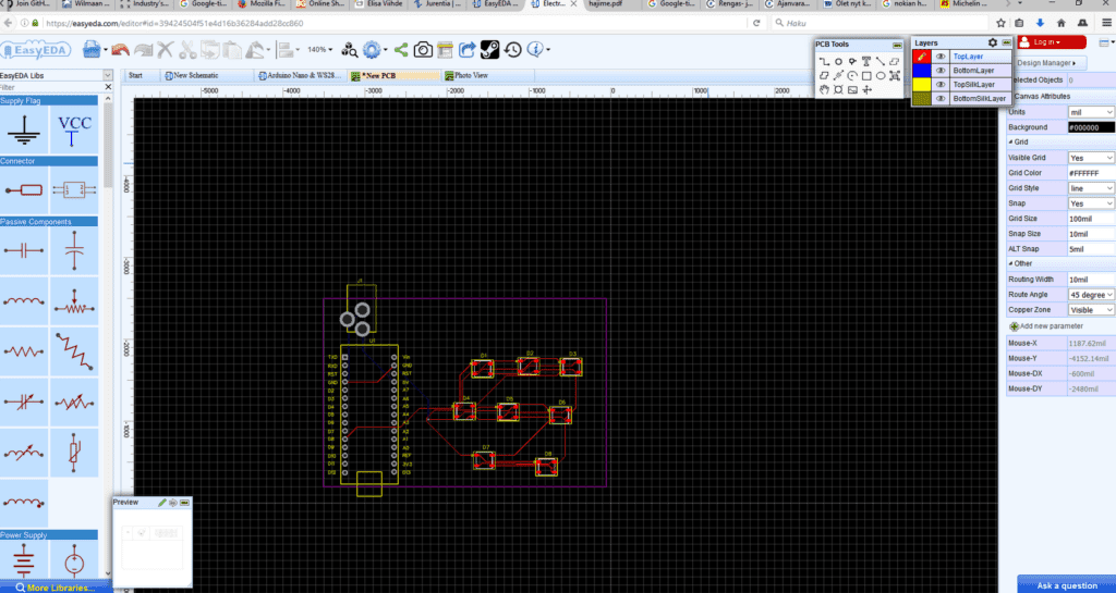
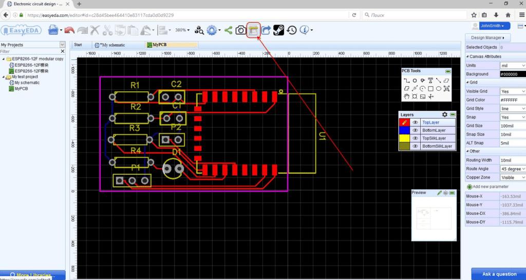
First, draw your music controlled led’s schematic on EasyEDA and click on “Convert project to PCB.” The next stage is placing the components; drag and drop the components too where you want them to be. Next draw a custom PCB outline; start by selecting the “BoardOutline ” opposite layer in the layers menu and clicking on the current custom outline. A good PCB layout is key to achieving an impressive outcome.
When you’re done creating an outline or a PCB layout, draw a copper area (mostly used GND) using the Copper Area properties menu. In creating this PCB layout, please pay attention to the gerber files. To identify these files, using EasyEDA PCB design editor is the best option.
The next thing is to start routing and you can do this with an auto router; the Auto Router function is the easiest way to do this. If you plan on mounting your PCB onto something, add some holes by clicking on the “Hole” tool in the tools dotted line. If possible, you can solder SMD components of the fabrication output together.
Next, add text or image and place the respective content in multiple layers from the tools menu. Now, finish the design by reviewing the finished product on the same function; to do that click on “Photo View.”
Who Needs EasyEDA?
EasyEDA is designed for professionals, hobbyists, and students who want to learn PCB design at the professional level. Also, if you want a free but highly efficient PCB design tool, you might want to get EasyEDA. With this, you can create a free account and use the online PCB editor and other features in the tools menu.
Is EasyEDA a Good PCB Design Tool?
EasyEDA is a completely free cloud-based CAD tool created for designing professional level PCBs using a built-in PCB ordering system. Compared with others, EasyEDA has the shortest learning curve and many readily available PCB footprints for nearly all single components and customized modules. Thousands of EasyEDA are already creating their own components, adding to and sharing the software’s library almost every day.
What Are the Features of EasyEDA?
EasyEDA comes with multiple features; it is the most utilized circuit simulation and development tool for many. Some of its features include:
- Easier and efficient circuit designing capabilities,
- Private and public projects sharing capabilities,
- Ability to develop a variety of open-source projects,
- Script support and API provision,
- PCB fabrication and components purchase,
- Digital project sharing,
- Themes setting,
- Documents recover at any level,
- Documents export in PNG, SVG, and PDF forms,
- Netlist export,
- Checking of design rules,
- Creating and editing footprint, and many more.
How do You Design with EasyEDA?
First, open the editor section in the software and choose what you want to create – whether components or footprints. Next, create new components and footprints and capture the schematics. When you have done that, use simulation procedure to verify circuits, after which you will run simulation. The last steps are the conversion of Schematic Layout to PCB and, finally, ordering PCBs.
How Can You Design Boards with EasyEDA?
Before you start placing the footprints, you need to first create a board outline. Go to the PCB tools palette and choose Arc and Track to track sizes and draw the outline in the board outline layer. This could be a bottom layer, copper layers, or cross lines. depending on the current outline or gerber file you are working with.
The tool will create a board for you while you convert the schematic to PCB. You can design following the blue line moving per time and use the correct pads and fill style or press delete to correct errors
How Do You Design the Circuit’s Schematic Plan with EasyEDA?
Start by clicking on the “New Schematic” option and choose all the components you need from the libraries section. Drag them from the left panel into the empty canvas and right click or press the “ESC” button to exit.
Next, drag the wire between components to establish copper connection between components. To change the component gas’s attributes, select the specific component and go to the right-side panel section to modify.
How Do You Do Circuit Simulation in EasyEDA?

After creating the schematic layout of the circuit, go to the top layer and click the green button to run the simulation. A pop-up window will appear; choose the type of simulation you want to run and click on “Run.” You can choose from AC analysis, transient, DC op pnt, DC transfer, or DC sweep simulation.
What is the Process for Converting a Project to PCB?
For project to PCB conversion, select the option “PROJECT TO PCT” in the schematic board. Any component in the schematic diagram without PCB traces will be distributed per PCB model board. Systematically organize the components; once you do this, the input and output will be at their respective terminals. Find the blue lines on the PCB board and then go ahead to print the PCB board.
How to Create a 4-Layer PCB Layout with EasyEDA and Hillmancurtis
Hillmancurtis is a PCB manufacturing service that helps users save time and turn their ideas into reality. First, you must have created an account on service EasyEDA; then start a new outline project, and draw and save the schematics.
Next, create an online PCB layout by clicking on “Convert to PCB” and start placing the components. When you are done, switch to your desired layer by clicking the “Copper Layer” drop box and selecting 4; then, select and route all the components.
What is the Best PCB Assembly Service in China?
Hillmancurtis is one of the best PCB assembly manufacturers in China, offering complete PCB assembly services and the appropriate tools menu. Its services include PCB manufacturing, fabrication, assembly, and desired components sourcing, among others. It is capable of providing partial and turn-key printed circuit board assembly services with 100% original components.
Conclusion
In this article, you have learned about EasyEDA as well as PCB designing, schematic diagram drawing, circuit simulation, and PCB layout conversion. EasyEDA is a free, easy-to-use, zero-install digital circuit simulator that makes designing complicated circuits very easy with the right properties menu for anyone who wants to use the component’s pin.
