Electrical PCB design is a crucial aspect of modern-day electronics. A printed circuit board (PCB) is the backbone of any electronic device as it connects all the components together. The design of a PCB is a complex process that involves various steps, including schematic capture, component placement, and routing.
The schematic capture is the first step in PCB design, where the engineer creates a visual representation of the circuit. This step involves the selection of components and their positioning on the board. Once the schematic is complete, the engineer moves on to the placement of components on the board. Component placement is a critical step as it affects the overall performance of the circuit. The engineer must consider factors such as signal integrity, thermal management, and mechanical constraints.
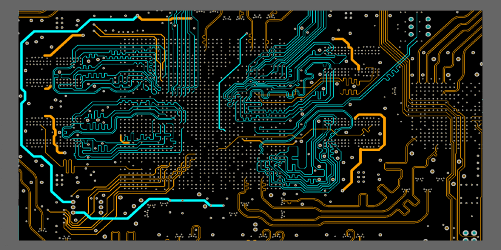
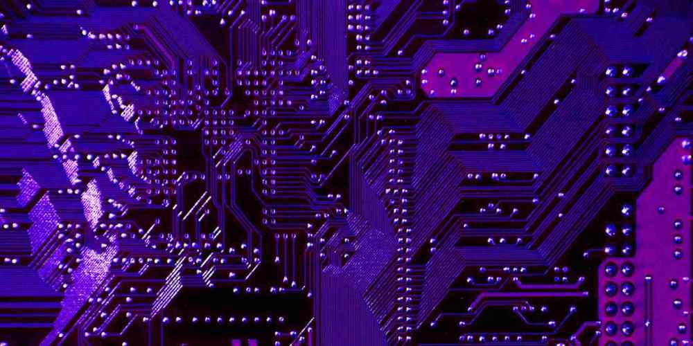
Routing is the final step in the PCB design process, where the engineer creates the physical connections between the components. The routing process involves the creation of copper traces that connect the components on the board. The engineer must ensure that the traces are of the correct width, length, and spacing to avoid signal interference and crosstalk. In conclusion, electrical PCB design is a complex process that requires a high level of skill and expertise. The design of a PCB can make or break the performance of an electronic device, making it a critical aspect of modern-day electronics.
Basics of Electrical PCB Design
Schematic Design
Schematic design is the first step in the electrical PCB design process. It involves creating a visual representation of the circuit using symbols to represent the components and lines to represent the connections between them. The schematic design should clearly show the functionality of the circuit and the relationship between the components.
When designing the schematic, it is important to consider the power requirements, signal flow, and component placement. The schematic should also include any necessary notes, such as component values or specific instructions for assembly.
PCB Layout Design
Once the schematic design is complete, the next step is to create the physical layout of the PCB. The layout design involves placing the components on the board and routing the connections between them. The layout should be optimized for signal integrity, power delivery, and manufacturability.
When designing the layout, it is important to consider the size and shape of the board, the placement of components, and the routing of traces. The layout should also include any necessary design rules and constraints, such as minimum trace widths and spacing.
Overall, the schematic and layout designs are critical components of the electrical PCB design process. A well-designed circuit can improve performance, reduce costs, and increase reliability. By following best practices and considering all aspects of the design, engineers can create high-quality PCBs that meet the needs of their applications.
Tools and Software for Electrical PCB Design
When it comes to designing electrical PCBs, there are a variety of tools and software available to help you create the best possible design. Here are two types of software that are essential for electrical PCB design:
Schematic Capture Software
Schematic capture software is used to create a diagram of the circuit that you want to design. This software allows you to add components, connect them together, and label them appropriately. Some popular schematic capture software include:
- Altium Designer
- Eagle PCB Design
- KiCad
PCB Layout Software
PCB layout software is used to take the schematic diagram and turn it into a physical PCB layout. This software allows you to place the components on the board, route the connections between them, and generate the necessary files for manufacturing. Some popular PCB layout software include:
- Altium Designer
- Eagle PCB Design
- KiCad
It’s important to note that different software packages have different strengths and weaknesses. For example, Altium Designer is known for its powerful design rule checking capabilities, while KiCad is known for being open source and free to use. Before selecting a software package, it’s important to research and compare different options to find the one that best fits your needs.
In conclusion, having the right tools and software is essential for creating a successful electrical PCB design. Schematic capture software and PCB layout software are two key types of software that are necessary for this process. By selecting the right software package, you can ensure that your design is accurate, efficient, and effective.
Design Considerations for Electrical PCB Design

When designing a printed circuit board (PCB) for electrical applications, there are several important considerations to keep in mind. These include component selection, signal integrity, and power integrity. By paying attention to these factors, you can ensure that your PCB design functions reliably and efficiently.
Component Selection
One of the most critical aspects of PCB design is selecting the right components for your circuit. You should consider factors such as the component’s size, cost, and performance characteristics. It’s also important to ensure that the components you choose are compatible with your PCB layout and can be soldered onto the board.
When selecting components, you should also consider their reliability and longevity. Choosing high-quality components can help prevent failures and ensure that your PCB design lasts for a long time.
Signal Integrity
Signal integrity is another crucial consideration in PCB design. This refers to the quality of the signals that are transmitted through the circuit. Poor signal integrity can result in data errors, noise, and other issues that can affect the performance of your design.
To ensure good signal integrity, you should pay attention to factors such as signal routing, trace impedance, and ground plane design. You should also consider using shielding and filtering techniques to reduce interference and noise.
Power Integrity
Power integrity is the third major consideration in PCB design. This refers to the quality of the power supply that is provided to the circuit. Poor power integrity can result in voltage drops, noise, and other issues that can affect the performance of your design.
To ensure good power integrity, you should pay attention to factors such as power routing, decoupling capacitors, and power plane design. You should also consider using voltage regulators and other techniques to stabilize the power supply and prevent voltage fluctuations.
In summary, when designing a PCB for electrical applications, it’s important to consider factors such as component selection, signal integrity, and power integrity. By paying attention to these considerations, you can ensure that your design functions reliably and efficiently.
Testing and Validation for Electrical PCB Design
Design Rule Checking
Design rule checking (DRC) is a crucial step in the PCB design process. It involves verifying that the design meets the rules and constraints specified by the manufacturer and industry standards. DRC helps to detect errors such as short circuits, open circuits, and other issues that could cause the PCB to malfunction or fail.
During the DRC process, the design software compares the design against a set of rules and constraints. These rules and constraints include minimum trace width, minimum clearance, and maximum via size. The software flags any violations, and the designer must correct them before proceeding with the design.
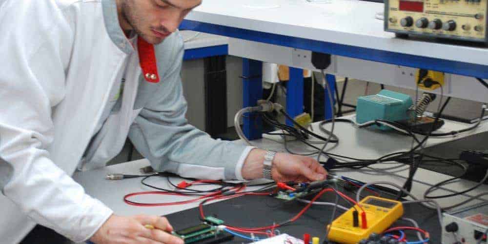
Electrical Testing
Electrical testing is another critical step in the PCB design process. It involves verifying that the PCB functions correctly and meets the required specifications. Electrical testing can be done using a variety of methods, including in-circuit testing (ICT), functional testing, and boundary scan testing.
In-circuit testing involves testing the components on the PCB while they are still mounted on the board. This type of testing can detect faults such as open circuits, short circuits, and incorrect component values. Functional testing, on the other hand, involves testing the PCB’s overall functionality. It is usually done after the PCB has been assembled.
Boundary scan testing is a type of testing that verifies the integrity of the interconnects between components on the PCB. It is particularly useful for detecting faults in complex designs that are difficult to test using other methods.
In conclusion, testing and validation are critical steps in the PCB design process. Design rule checking and electrical testing help to ensure that the PCB functions correctly and meets the required specifications. By following these steps, designers can reduce the risk of errors and ensure that the PCB performs as expected.
Advanced Techniques for Electrical PCB Design
High-Speed Design
High-speed design is a critical aspect of PCB design. It involves designing circuits that can operate at high frequencies without signal distortion. Here are some advanced techniques for high-speed design:
-
Impedance Control: Controlling the impedance of transmission lines is crucial for high-speed design. Matching the impedance of the source, transmission line, and load can help reduce signal reflections and improve signal integrity.
-
Grounding Techniques: Proper grounding is essential for high-speed design. Ground planes, split planes, and stitching vias can help reduce noise and improve signal integrity.
-
Crosstalk Mitigation: Crosstalk can occur when signals on one trace interfere with signals on another trace. Techniques such as spacing, shielding, and termination can help reduce crosstalk.
RF Design
RF design involves designing circuits that operate at radio frequencies. It requires careful consideration of impedance, signal integrity, and noise. Here are some advanced techniques for RF design:
-
RF Component Selection: Choosing the right components for RF circuits is critical. Components such as filters, amplifiers, and mixers must be carefully selected to meet the desired specifications.
-
RF Layout: The layout of an RF circuit can significantly impact its performance. Techniques such as grounding, shielding, and trace routing can help reduce noise and improve signal integrity.
-
EMI/EMC Mitigation: EMI/EMC can cause interference with RF circuits. Techniques such as filtering, shielding, and grounding can help reduce EMI/EMC and improve performance.
In conclusion, high-speed and RF design are critical aspects of PCB design. Advanced techniques such as impedance control, grounding, crosstalk mitigation, component selection, layout, and EMI/EMC mitigation can help improve signal integrity and reduce noise.
