Electronics PCB manufacturing is the process of creating printed circuit boards that are used in electronic devices. This process involves designing the circuit, creating a layout, and then manufacturing the board. PCBs are essential components in modern electronics, and they enable the creation of complex electronic devices that are smaller, faster, and more efficient than ever before.
The manufacturing of PCBs involves several steps, including design, layout, printing, etching, drilling, and assembly. The design process involves creating a schematic for the circuit, which is then translated into a layout that can be printed onto the board. The printing process involves transferring the layout onto the board using a special printer, and then etching away the unwanted copper to create the circuit. The board is then drilled to create holes for the components, and the components are assembled onto the board. The final product is a fully functional PCB that can be used in a wide range of electronic devices.
PCB Manufacturing Process
Designing the PCB
The first step in PCB manufacturing is designing the PCB. This involves creating a schematic diagram of the circuit and then designing the layout of the PCB. There are many software tools available for PCB design, such as Eagle, Altium, and KiCAD. The design should take into account the size and shape of the PCB, the placement of components, and the routing of traces.
Printing the PCB
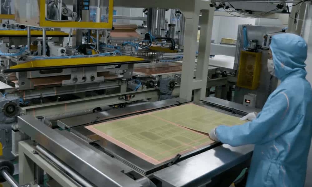
Once the design is complete, the next step is to print the PCB onto a substrate. This is typically done using a special printer that prints the design onto a sheet of copper-clad laminate. The printer uses a special ink that resists etching, allowing the design to be transferred to the copper layer.
Etching the PCB
After the design has been printed onto the substrate, the next step is to etch the PCB. This involves removing the unwanted copper using a chemical solution. The etching process can be done manually or using a specialized machine. Once the etching is complete, the remaining copper forms the traces and pads of the PCB.
Drilling Holes
After the PCB has been etched, the next step is to drill holes for the components. This is typically done using a specialized drilling machine that can drill precise holes in the PCB. The holes are then plated with copper to provide a conductive layer for the components.
Plating and Coating
After the holes have been drilled, the next step is to plate and coat the PCB. This involves adding a layer of metal to the exposed copper traces and pads to protect them from corrosion. The PCB is then coated with a layer of solder mask to protect the traces and pads from accidental short-circuits.
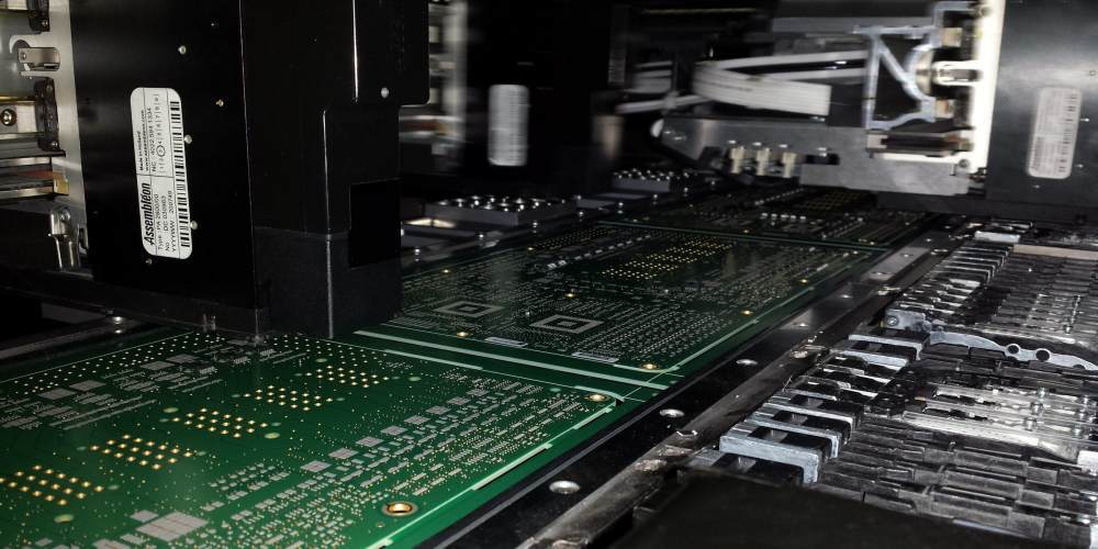
Soldering Components
Once the plating and coating are complete, the next step is to solder the components onto the PCB. This involves placing the components onto the PCB and then heating them to melt the solder, which then flows onto the pads to create a strong electrical connection.
Testing the PCB
The final step in PCB manufacturing is testing the PCB. This involves checking the electrical connections between the components to ensure that the PCB is functioning correctly. There are many different testing methods available, such as visual inspection, continuity testing, and functional testing.
In conclusion, PCB manufacturing involves several steps, each of which is critical to the final product. By following a well-defined process and using specialized tools and techniques, it is possible to create high-quality PCBs that meet the needs of a wide range of applications.
Types of PCBs

When it comes to electronics PCB manufacturing, there are several types of PCBs available. Each type has its own set of benefits and drawbacks, making it important to choose the right type for your specific application.
Single-Sided PCBs
Single-sided PCBs are the most basic type of PCB. They consist of a single layer of conductive material, typically copper, on one side of an insulating material. This type of PCB is commonly used in simple electronic devices, such as calculators and toys.
Double-Sided PCBs
Double-sided PCBs have conductive material on both sides of the insulating material, allowing for more complex circuit designs. These PCBs are commonly used in applications such as power supplies and amplifiers.
Multi-Layer PCBs
Multi-layer PCBs have multiple layers of conductive material separated by insulating material. This allows for even more complex circuit designs and can help reduce the size of the PCB. Multi-layer PCBs are commonly used in smartphones, computers, and other high-tech devices.
Rigid PCBs
Rigid PCBs are made from a solid, inflexible material such as fiberglass or plastic. They are commonly used in applications where the PCB will not be subjected to bending or flexing.
Flexible PCBs
Flexible PCBs are made from a flexible material such as polyimide. They are commonly used in applications where the PCB will be subjected to bending or flexing, such as in wearable technology or medical devices.
Rigid-Flex PCBs
Rigid-flex PCBs combine the benefits of both rigid and flexible PCBs. They have both rigid and flexible sections, allowing for more complex circuit designs that can be used in a variety of applications.
In summary, there are several types of PCBs available, each with its own set of benefits and drawbacks. It is important to choose the right type of PCB for your specific application to ensure optimal performance and reliability.
Materials Used
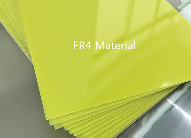
Copper Clad Laminate
Copper clad laminate (CCL) is the base material used in PCB manufacturing. It is composed of a thin layer of copper foil laminated to a non-conductive substrate. The substrate is typically made of fiberglass or paper reinforced phenolic resin. The thickness of the copper foil can vary, but 1 oz copper (35 µm) is most commonly used.
Solder Mask
Solder mask is a protective layer applied to the PCB surface to protect the copper traces from oxidation and contamination during soldering. It is typically green or red in color, but other colors are available. The solder mask is applied in a liquid form and then cured under UV light.
Silkscreen
Silkscreen is a layer of ink applied to the PCB surface to indicate component placement, part numbers, and other important information. It is typically white in color, but other colors are available. The silkscreen is applied using a stencil and then cured under UV light.
Copper Foil
Copper foil is used to create the conductive pathways on the PCB surface. It is typically laminated to the CCL substrate using heat and pressure. The thickness of the copper foil can vary, but 1 oz copper (35 µm) is most commonly used.
Adhesive
Adhesive is used to bond the different layers of the PCB together. It is typically a thermosetting epoxy resin that is applied as a liquid and then cured under heat and pressure.
In summary, copper clad laminate, solder mask, silkscreen, copper foil, and adhesive are the main materials used in PCB manufacturing. Each material plays a crucial role in creating a reliable and high-quality PCB.
Quality Control in PCB Manufacturing
Visual Inspection
Visual inspection is an important step in quality control during PCB manufacturing. It involves checking the board for any defects or irregularities that may have occurred during the manufacturing process. The inspector checks for any physical damage, such as scratches or cracks, and also checks for any deviations from the design specifications.
Electrical Testing
Electrical testing is another crucial step in quality control. This involves testing the board to ensure that it meets the electrical specifications and functions properly. The board is tested for continuity, shorts, and open circuits. This step helps to ensure that the board will work as intended when it is installed in the final product.
X-Ray Inspection
X-ray inspection is a non-destructive testing method used to detect any internal defects in the board. It is particularly useful for detecting defects that are not visible through visual inspection. X-ray inspection can detect issues such as voids in solder joints, misaligned vias, and other defects that can impact the reliability and performance of the board.
In conclusion, quality control is an essential part of PCB manufacturing. Visual inspection, electrical testing, and X-ray inspection are all important steps in ensuring that the board meets the design specifications and functions properly. By following these steps, manufacturers can produce high-quality PCBs that meet the needs of their customers.
Advancements in PCB Manufacturing
Automation
Advancements in automation have revolutionized PCB manufacturing. Automated machines can now perform a wide range of tasks such as drilling, routing, and testing. This has significantly reduced the time and cost required for PCB production. Automation has also improved the accuracy and precision of PCB manufacturing, resulting in higher quality products.
Miniaturization
Miniaturization is another significant advancement in PCB manufacturing. With the increasing demand for smaller and more compact devices, PCBs have become smaller and more densely packed. This has been made possible by advancements in manufacturing techniques such as laser drilling, which can create smaller holes with higher precision. As a result, PCBs can now be used in a wide range of applications, from medical devices to smartphones.
3D Printing
3D printing is a relatively new technology that has been applied to PCB manufacturing. With 3D printing, it is now possible to create complex PCB designs that were previously impossible to produce using traditional manufacturing methods. 3D printing also allows for the creation of custom-shaped PCBs, which can be used in a wide range of applications.
Flexible Electronics
Flexible electronics is another area where advancements in PCB manufacturing have been made. With the increasing demand for wearable devices, PCBs that can bend and flex have become more important. Flexible PCBs are made using specialized materials and manufacturing techniques, which allow them to bend and flex without breaking. This has opened up new possibilities for the development of wearable devices, such as smartwatches and fitness trackers.
In summary, advancements in automation, miniaturization, 3D printing, and flexible electronics have revolutionized PCB manufacturing. These advancements have led to faster, more accurate, and higher quality production of PCBs. As technology continues to advance, we can expect further improvements in PCB manufacturing, leading to even more innovative and exciting applications.
