FPC PCB is a compound term coined from two words that encompass what the term is all about. FPC is an abbreviation for flexible printed circuit and PCB means printed circuit board. Another way is to refer to this complex term as a flexible printed circuit board.
FPC is a type of circuit board and to understand it better you’ll need a robust understanding of PCBs, so let’s have a looks at it.
What is a Printed Circuit Board?
In electrical engineering, a PCB (also known as a printed wiring board or PWB) is a medium used to link electronic components together in a specific way that complies with design. Fiberglass is a typical PCB Media. For electrical conductivity, it typically has a metallic circuit or tracks printed or etched on it. These printed tracks are sometimes made of copper.
Almost all of the electrical items we use daily use a PCB. It can also be found in larger equipment like military weapons, airplanes, and satellites as well as in gadgets like mobile phones, tablets, TVs, computers, laptops, keyboards, and mice.
This piece of electrical design is very common and quite important in modern engineering times. It allows for the manufacture of compact devices without the complexity of wiring and interconnectivity between numerous small components.
The manufacture of PCBs is now automated in something called electronic design automation. This automation is important because present-day circuit boards sometimes have thousands of connections. Automation eliminates the chances of error.
Types of Printed Circuit Boards
There are varying types of printed circuit boards in the electronics industry based on certain factors like design, production, application, and function, and before you pick one for use, you have to consider some factors like the stress to which the manufactured device will be subjected.
There are six major types. the space required and available for the PCB in the device, and the stability of the device.
Single Sided PCB
The most typical sort of printed circuit board is a single-sided PCB. Above the substrate, it has a solitary copper layer that conducts electricity.
On one side of the board, where the electrical components are soldered or positioned, the fully etched circuit is visible. Because there is only one conducting layer on these boards, the conductive channels are quite large and cannot overlap.
These PCBs can accommodate low-density design needs. Basic and inexpensive electrical/electronic devices including FM radios, power supplies, LED lighting boards, calculators, and timing circuits employ single-sided printed circuit boards (PCBs).
This type of circuit board is quite cost-effective to mass produce, and automation makes the production and designs easy and seamless. This type of circuit board is the most basic and as such, it is the easiest to repair, in the case where electronic components are damaged in the device or on the circuit board.
Double Sided PCB
When a printed circuit board (PCB) is double-sided, both the top and bottom sides of the board are covered with a very thin layer of conductive material. Copper is the metal that the vast majority of producers want to work with the most.
Metal components can be connected from one side to the other using holes drilled into the circuit board. Through-hole technology or surface mount technology are two mounting techniques used by these PCBs to link the circuitry on each side.
With through-hole technology, lead components are inserted into the circuit board’s pre-drilled holes and then soldered to pads on the opposing sides. With surface mount technology, electrical components are precisely positioned on the surface of circuit boards.
In the PCB industry, double-sided PCBs are used in some pretty common devices like cell phones, UPS devices, and amplifiers. Double-sided PCBs allow manufacturers to create more compact and smaller devices. In the production of such devices, manufacturers can use both faces of the circuit board instead of having to design the device to accommodate two boards.
This way the cost of production is greatly reduced. Although the design of the double-sided board is a bit more complex than the single-sided board, automated design makes the design process efficient and fast. This type of PCB can be used for more complex electronic systems and it is more flexible.
Multilayer PCBs
On a printed circuit board with several layers, there are more than two copper layers. In general, any board that has at least three conducting layers is considered to fall under this category.
In the “sandwich” architecture of a multilayer printed circuit board (PCB), there are many conductive layers that are on both sides of the board. These layers are separated by an equal number of sheets of insulating material.
To make certain that there are no air gaps and that the finished PCB assembly is appropriately stable, all of these must be fused and laminated together at high pressures and high temperatures.
Computers, laptops, mobile phones, tablets, medical equipment, GPS trackers, and several other more complicated circuits and gadgets employ multi-layer printed circuit boards (PCBs). This type of circuit board has a high-level design, is compact, and is more robust, making it perfect for high-speed circuits.
Rigid PCBs
Rigid printed circuit boards are a form of a rigid board that cannot be folded or twisted in any way, as suggested by the name of this type of board. Due to the hard substrate that acts as the board’s basis, it has the stiffness and strength of metallic circuits or tracks that have been printed on it.
They are made up of many layers, such as a silkscreen layer, a solder mask layer, a substrate layer, and a copper layer, which are glued together with adhesive and heat.
Rigid printed circuit boards can be any of these, depending on the needs, even if some circuit boards are either single-sided, double-sided, or multi-layered. They can’t be altered or changed after they’ve been made, though.
This type of PCB has quite a long list of advantages, some of which is how that they are very easy to diagnose and repair and they produce low electric noise. This type of circuit is lightweight, compact, and can absorb vibrations. They are also economical to produce.
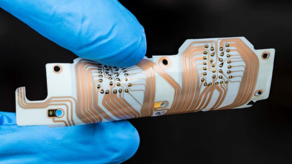
Rigid-Flex PCBs
This type of circuit board is a hybrid that combines parts from rigid circuit boards and flexible circuit boards. As a result, during the production process, it is frequently molded into a flexed shape or curve and may be folded or continually bent.
The flexible portion of the board is typically used to connect fixed boards. This makes it possible to employ boards that are more compact and have narrower conductor lines. When flexible printed circuits are utilized for interconnections rather than bulky, heavy connectors, rigid-flex printed circuit boards become noticeably lighter.
Rigid-flex PCB designs are a little more difficult because these boards can be folded or twisted to take on the required shape for the product and are constructed through the three-dimensional assembly.
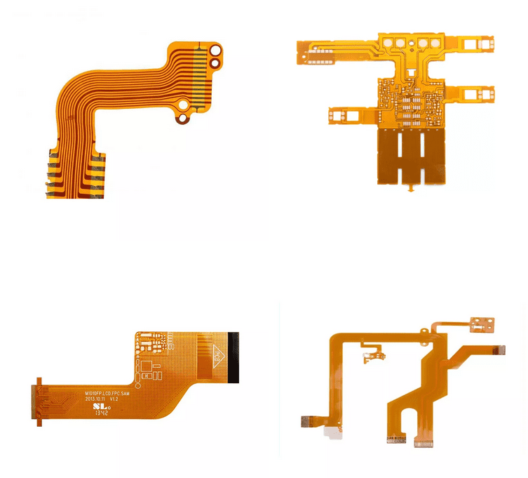
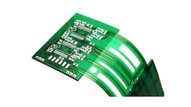
Flexible Printed Circuit Boards
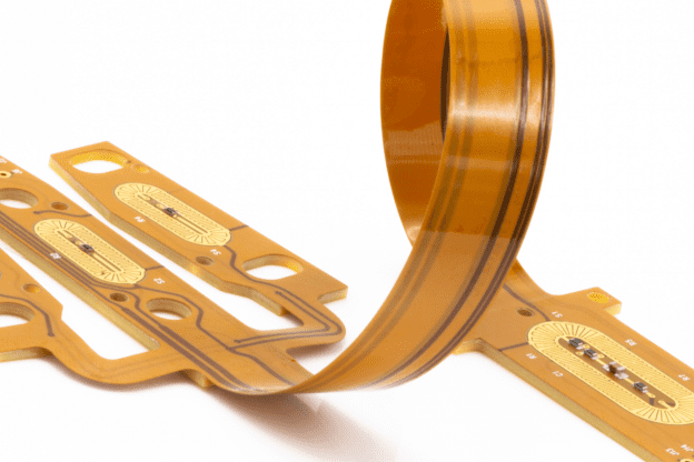
An insulating polyimide membrane with printed circuit designs makes up normal flexible circuit boards or Flex PCBs. Only the circuit layout conducts because polyimide is an insulator, completing the path. One top quality of these flex circuits is that they
Similar to the rigid PCB’s “solder mask,” flex PCBs have a thin “cover layer” that shields the circuit from electromagnetic interference.
Nowadays, flex PCBs are widely used in medical and smartphone applications, particularly where the circuit must resist significant temperature changes while preserving flexibility.
There are various reasons why flexible printed circuits are seen as flexible. The fact that their circuitry can be modified to work with the product itself is the most obvious of all of them.
This is advantageous, especially when considering factors like sustainability, durability, lightweight, and flexibility. Conventional boards cannot satisfy the requirement of being strong, delicate, and powerful all at once.
Due to its propensity to easily oxidize, copper commonly has its exposed surfaces coated with a layer of protection; due to its conductivity and environmental resistance, gold or solder are the two most popular options.
A dielectric material is utilized to shield the circuitry from oxidation or electrical shorting in non-contact locations.
Composition of an FPC PCB material
Substrate
The base substrate material is the most crucial component of a rigid or flexible PCB. It serves as the foundation for the entire PCB.
FR-4 is often used as the substrate material for inflexible printed circuit boards (PCB). Nevertheless, PET (polyester) and Polyimide (PI) film are the substrate materials that are utilized in flexible printed circuits the majority of the time. There are various polymer films available, such as polyethylene nphthalate (PEN), polytetrafluoroethylene (PTFE), and aramid.
The most often utilized material for Flex PCBs is Polyimide (PI). It possesses remarkable electrical qualities, excellent heat resistance, excellent chemical resistance, and excellent tensile strength, and is stable across a wide range of operating temperatures.
Unlike other thermosetting resins, it can maintain its flexibility even after thermal polymerization. Poor grip strength and significant moisture absorption, however, are drawbacks of PI resin.
However, PET (Polyester) resin has strong electrical and mechanical properties despite having low heat resistance, making it unsuitable for direct soldering. Another substrate, PEN, performs at a medium level, better than PET but not better than PI.
LCP is the most used substrate material in Flex PCBs today. This is because it maintains all of PI’s features while overcoming the drawbacks of the PI substrate. The LCP’s dielectric constant at 1GHz is 2.85 and it has excellent moisture resistance.
Due to this, it is widely used in high-speed digital and RF circuits. The melted form of LCP (TLCP) is easily recyclable and may be pressed and injection molded to create a flexible PCB substrate.
Resin
The resin that holds the copper foil and substrate material together is another crucial component of FPCs. The resin may be acrylic resin, modified epoxy resin, PI resin, or PET resin.
The sandwich known as laminate is made up of substrate materials, copper foils, and resin. This laminate often referred to as Flexible Copper Clad laminate is created by using an automatic press to apply high pressure and temperature to the sandwich stack in a controlled environment.
The modified epoxy resin and acrylic resin, out of the aforementioned resin kinds, offer the strongest adhesive qualities. Although these offer the strongest adhesion, they have poor electrical and thermal performance and reduce the overall stability of the FPC.
The use of the 2-layer FCCL without glue is the answer to this issue. The 2L FCCL has excellent electrical characteristics, a high level of heat resistance, and good dimensional stability, but its production is challenging and expensive.
Copper Foil
Copper is another component of flex PCBs. Copper is used as a conducting material to fill the PCB tracks, pads, and holes. The fact that copper is an electrical conductor is well known.
How to print these copper traces on PCB is the crux. On a 2 Layer Flexible Copper Clad Laminate substrate, copper can be deposited in 2 different methods.
Lamination is the second procedure, and electroplating is the first. While the lamination method requires adhesives, the electroplating method does not.
Electroplating
The electroplating method is preferable to the lamination method in the production of a flexible printed circuit with super thin thickness. Sputtering refers to the wet or dry electroless plating procedure used to deposit copper on a PI layer.
The copper seed layer created by this electroless plating is extremely thin. The following stage involves electroplating to add another layer of copper.
The thin seed layer of copper is followed by a second, somewhat thicker layer of copper. Without the use of adhesives, the entire procedure produces a solid bond between PI and copper. Flexible circuit board reliability is significantly increased by this technology, which is also inexpensive.

Lamination
Here, a coverlay is used to laminate a very thin copper foil onto the PI substrate. The coverlay is a sophisticated film made from polyimide with a thermosetting epoxy adhesive.
This coverlay adhesive has outstanding electrical insulating qualities even when bent, excellent heat resistance, it is fire retardant, and it has gap-filling capabilities. Photo Imageable Coverlay (PIC) is a unique variety of coverlay.
This kind of coverlay has outstanding flexibility resistance, excellent binding force, and is environmentally friendly. PIC’s poorer thermal resistance and low glass transition temperature, however, are a drawback.
The produced copper foil is of two types, electro-deposited copper and rolled annealed copper. The electrodeposited copper has better conductivity, but the rolled annealed copper has better extension properties than the electrodeposited one.
Conclusion
There’s no denying that the world of technology and engineering has seen great improvements since the advent of flexible circuit boards. The flexible substrate which is the flexible material in these flex circuit boards has made the production of many compact and small devices possible over the past few years like the world has never seen before.
Everything from electric toy cars to high-end military weapons is a product of this amazing invention. With more exploration and discovery in science, tech, and engineering, the world of PCBs will produce more for human consumption.
