A printed circuit board (PCB) is a fundamental component of electronic devices. It connects and supports electronic components while providing electrical pathways. PCBs are used in a wide range of applications, including audio amplifiers. One popular type of audio amplifier is the OCL 150 Watt amplifier, which is known for its high power output and excellent sound quality.
Layout design is a crucial part of PCB design, especially for audio amplifiers. It involves arranging components and traces on the board to ensure optimal performance and reduce interference. In the case of the OCL 150 Watt amplifier, the layout design must be carefully planned to ensure that the amplifier operates at its full potential. This includes minimizing noise, reducing distortion, and ensuring proper heat dissipation. In this article, we will explore the layout design of the OCL 150 Watt amplifier PCB and provide tips for designing an optimal layout.
Fundamentals of OCL 150 Watt Amplifier
An OCL (Output Capacitor-Less) amplifier is a type of power amplifier that does not require an output capacitor to block DC voltage. It is a popular choice for high power audio amplifiers due to its simplicity and low cost. In this section, we will discuss the fundamental principles of an OCL 150 watt amplifier.
The OCL 150 watt amplifier is a class-AB amplifier that uses a pair of complementary output transistors to amplify the input signal. The amplifier circuit consists of three stages: the input stage, the driver stage, and the output stage.
The input stage is responsible for amplifying the input signal to a level that can be further amplified by the driver stage. The driver stage then amplifies the signal further and drives the output stage. The output stage is responsible for delivering the amplified signal to the load.
The OCL 150 watt amplifier has a high power output and can drive low impedance loads. The output stage is designed to handle high currents and voltages, which makes it suitable for driving large speakers.
One of the advantages of an OCL amplifier is its low distortion. The absence of an output capacitor eliminates the need for a coupling capacitor, which can introduce distortion. The OCL amplifier also has a high damping factor, which means it can control the movement of the speaker cone more accurately.
In summary, the OCL 150 watt amplifier is a class-AB amplifier that uses a pair of complementary output transistors to amplify the input signal. It has a simple and low-cost design, high power output, low distortion, and high damping factor.
PCB Layout Design Basics
When designing a PCB layout for an OCL 150 watt amplifier, there are some basic principles to keep in mind. A well-designed PCB layout can help reduce noise and distortion, improve thermal management, and minimize the risk of electrical shorts.
Component Placement
The placement of components on the PCB can have a significant impact on the performance of the amplifier. To reduce noise and interference, it is important to keep sensitive components, such as the input and output stages, away from noisy components like power supplies and transformers. Additionally, components that generate heat, such as power transistors, should be placed in areas with good thermal management, such as near heat sinks or cooling fans.
Trace Routing
The routing of traces on the PCB can also have a significant impact on the performance of the amplifier. For example, it is important to keep high-current traces, such as those that connect the power supply to the amplifier, as short and wide as possible to minimize resistance and voltage drops. Additionally, it is important to keep signal traces away from noisy components and power traces to reduce interference and noise.
Grounding
Proper grounding is essential for the performance of the amplifier. A good grounding scheme should provide a low-impedance path for current to flow back to the power supply, while minimizing ground loops and noise. One common approach is to use a star grounding scheme, where all ground connections are made at a single point to minimize ground loops.
PCB Design Tools
There are many PCB design tools available that can help simplify the process of designing a PCB layout for an OCL 150 watt amplifier. These tools can help with tasks such as component placement, trace routing, and grounding, and can also provide simulations and analysis to help optimize the performance of the amplifier. Some popular PCB design tools include Eagle, Altium, and KiCad.
Amplifier Circuit Design

The OCL 150 Watt amplifier is designed to deliver high-quality sound with low distortion. The circuit is based on a dual power supply and uses a symmetrical layout to minimize noise and distortion.
The amplifier circuit consists of two main stages: the pre-amplifier and the power amplifier. The pre-amplifier is responsible for amplifying the input signal, while the power amplifier is responsible for driving the speakers.
The pre-amplifier stage uses a dual op-amp IC to amplify the input signal. The op-amp is configured as a non-inverting amplifier with a gain of approximately 10. The pre-amplifier also includes a tone control circuit, which allows the user to adjust the bass and treble frequencies.
The power amplifier stage uses a pair of complementary transistors to drive the speakers. The transistors are arranged in a Class AB configuration, which provides high efficiency and low distortion. The power amplifier also includes a protection circuit, which prevents the amplifier from being damaged in the event of a short circuit or overload.
To ensure the stability and reliability of the amplifier circuit, it is recommended to use high-quality components and to follow the layout guidelines provided in the schematic. The layout should be symmetrical and the ground plane should be connected to the chassis ground to minimize noise and hum.
Overall, the amplifier circuit design is straightforward and well-suited for DIY enthusiasts and audio professionals alike. With careful attention to detail and good quality components, the OCL 150 Watt amplifier can deliver high-quality sound with low distortion and excellent performance.
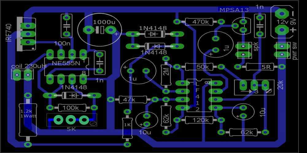
PCB Layout for OCL 150 Watt Amplifier
When designing a printed circuit board (PCB) for an OCL 150 Watt amplifier, it is important to pay attention to component placement, trace routing, and grounding strategies. These factors can greatly impact the performance and reliability of the amplifier.
Component Placement
Careful component placement is essential for an efficient and reliable amplifier. The placement of components should be done in a way that minimizes the length of traces and reduces the possibility of interference. It is important to keep the input and output circuits separated to avoid crosstalk.
Here are a few guidelines for component placement:
- Keep the input and output circuits separated.
- Place the power supply components near the power input.
- Place the heat sink and output transistors in a way that allows for efficient heat dissipation.
- Place the input signal components (such as capacitors and resistors) as close to the input connector as possible.
Trace Routing
Trace routing is the process of connecting the components on the PCB with traces. The routing should be done in a way that minimizes the length of the traces and reduces the possibility of interference. It is important to keep the input and output circuits separated to avoid crosstalk.
Here are a few guidelines for trace routing:
- Keep the input and output circuits separated.
- Use wide traces for the power supply and output circuits to minimize resistance and reduce heat dissipation.
- Use short traces for the input signal components to reduce noise and interference.
- Avoid sharp bends in the traces as they can cause reflections and signal degradation.
Grounding Strategies
Grounding is an important aspect of PCB design. It is important to have a solid and low impedance ground plane to reduce noise and interference. The ground plane should be connected to the chassis ground to reduce the possibility of ground loops.
Here are a few guidelines for grounding:
- Use a single point ground to minimize ground loops.
- Connect the ground plane to the chassis ground to reduce the possibility of ground loops.
- Use a low impedance ground plane to reduce noise and interference.
- Keep the ground plane away from the input and output circuits to avoid crosstalk.
By following these guidelines, you can create a reliable and efficient PCB layout for an OCL 150 Watt amplifier.
PCB Manufacturing Process

The manufacturing of a PCB for an OCL 150 Watt amplifier involves several steps. The process starts with the design of the PCB layout using software such as Eagle or Altium Designer. Once the design is complete, the layout is printed onto a special film, which is then used to transfer the design onto a copper-clad board.
The next step is to etch the board using a chemical process. A mask is applied to the board to protect the copper traces that make up the circuit from the etching solution. The exposed copper is then dissolved away, leaving only the traces behind.
After the etching process, the board is cleaned and drilled to create the holes for the components. The holes are then plated with a thin layer of copper to ensure good electrical contact between the component leads and the traces.
The board is then covered with a layer of solder mask, which protects the traces and pads from oxidation and provides a uniform surface for the application of solder. The solder mask is cured using ultraviolet light.
Finally, the board is silk-screened with component designators and other information to aid in assembly. The finished PCB is now ready for the placement of components and soldering.
Overall, the manufacturing process for a PCB is a precise and intricate process that requires careful attention to detail and a thorough understanding of the underlying principles. With the right tools and techniques, however, it is possible to create high-quality PCBs that meet the exacting standards required for an OCL 150 Watt amplifier.
Testing and Troubleshooting
After assembling the PCB amplifier, it is important to test and troubleshoot the circuit to ensure proper functionality. Here are some steps to follow:
-
Visual Inspection: Before testing, inspect the PCB for any visible defects, such as solder bridges or broken traces. Make sure all components are properly seated and oriented.
-
Power Supply Test: Connect the amplifier to the power supply and check the voltage levels at various points in the circuit using a multimeter. Verify that the voltage levels are within the expected range.
-
Signal Test: Connect a signal source, such as an audio signal generator, to the input of the amplifier and measure the output using an oscilloscope. Verify that the output waveform is clean and undistorted.
-
Load Test: Connect a load, such as a speaker, to the output of the amplifier and measure the output using an oscilloscope. Verify that the output waveform is clean and undistorted and that the amplifier can deliver the expected power output.
If any issues are found during testing, troubleshoot the circuit by checking each component and connection for proper values and continuity. Common issues include incorrect component values, faulty solder joints, and broken traces.
In summary, proper testing and troubleshooting are crucial to ensure the PCB amplifier functions as intended. By following these steps and thoroughly checking the circuit, any issues can be identified and resolved to achieve optimal performance.
Safety Precautions

When working on a PCB amplifier, it is important to take certain safety precautions to avoid injury or damage to the equipment. Here are some important safety measures to keep in mind:
-
Disconnect the power supply: Before starting work on the amplifier, always make sure to disconnect the power supply to avoid electric shock.
-
Wear safety gear: Always wear safety glasses and gloves when handling electronic components to avoid injury.
-
Work in a well-ventilated area: Soldering and other electronic work can release fumes that can be harmful if inhaled. Make sure to work in a well-ventilated area to avoid any health risks.
-
Avoid static electricity: Static electricity can damage electronic components, so make sure to ground yourself before handling any components. Use an anti-static wrist strap or mat to avoid any static buildup.
-
Use the right tools: Make sure to use the right tools for the job. Using the wrong tools can damage the equipment or cause injury.
-
Read the instructions: Always read the instructions carefully before starting work on the amplifier. Following the instructions will ensure that the amplifier is built correctly and safely.
By following these safety precautions, you can ensure that your PCB amplifier is built safely and correctly.
Conclusion

In conclusion, designing a PCB layout for an OCL 150 Watt amplifier requires careful consideration of various factors. The layout should be designed in such a way that it minimizes noise and distortion while maximizing the efficiency of the amplifier.
Throughout this article, we have discussed various tips and techniques for designing a PCB layout for an OCL 150 Watt amplifier. We have covered topics such as component placement, power supply design, and grounding techniques.
It is important to note that the success of the PCB layout will depend on the quality of the components used and the skill of the designer. A well-designed PCB layout can significantly improve the performance of the amplifier, while a poorly designed layout can result in a loss of fidelity and increased noise.
Overall, designing a PCB layout for an OCL 150 Watt amplifier is a complex process that requires careful consideration of various factors. However, with the right knowledge and techniques, it is possible to design a layout that results in a high-quality amplifier with minimal noise and distortion.
