The list of components to be used in designing a PCB is called the Netlist. In case you are looking to use one of these files, wondering what the difference is between it and the schematic and some other questions you may have – we try to answer them in this article.
An Overview of PCB Files
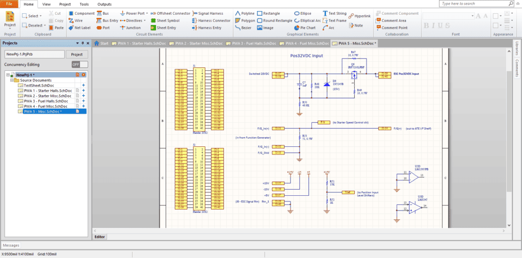
The design and or configuration of Printed Circuit Boards (PCBs) have improved over the years. The files used for this purpose have also been classified, based on the specifics they carry.
Today, you can use one file to describe the components to be bought for the PCB design and another file to outline where these components are to be placed on the board.
Thus, the essence of such files cannot be ruled out of the equation. It is also the reason why we want to describe what the Netlist file format is and how it impacts the PCB design.
What is Netlist in PCB Design?
The simplest way to understand this term is by going back to the basics. The terms are “net” and “list.”
Generally, the word or term, “net,” when used in the PCB industry, refers to the connection established between two or multiple electronic components. On the other hand, the word “list” refers to the itemization of items.
Thus, collecting the two terms together gives us a “list of connected electronic components.” Therefore, the Netlist file refers to the connectivity or connection of the electronic components in a circuitry.
PCB Netlist file is commonly presented in a textual format, which highlights the catalogue of electronic components in the circuitry and the connections going with them.
Why Use PCB Netlist File?
With several types of file formats out there for PCB design, why should you use the Netlist? Manufacturers prefer it for a wide range of reasons, including:
1. Incorrect Connection Detection
As a network of the different connected components, the PCB Netlist file helps the PCB manufacturer to find out the incorrect or missing connections. Ordinarily, this could have gone unnoticed only to resurface at the end of the design, thereby, leading to extra expenses to fix the issue.
By using the Netlist during the design, it becomes easier to detect these missing connections and have them filled up before the final design.
The easiest way to detect the missing connections is by putting the PCB to a series of electrical tests.
2. Schematic Verification
The PCB design may become error-filled, if the schematics’ specifications are not followed to the latter. By using the schematic Netlist, it is easier to verify and validate that the specifics of the schematics were followed to the latter.
There are two major ways to make this verification:
- By making sure that the final set of output files for the PCB match the Netlist. This also goes both ways, as the Netlist needs to match the specifications of the schematics.
- You can also use the Netlist file to compare the connection data with the information provided on the schematic file.
3. Final Design Considerations
To be on a safer side, PCB manufacturers prefer using the PCB Netlist file to compare with the schematics. This comes in handy for the production of the circuit board, as per the exact specifications.
Compositions of the PCB Netlist File
Several elements go into making the Netlist for a PCB. The following are some of the pieces of information you can find inside it:
Net Labels
This refers to the name given to the network (net) in the PCB’s schematic.
Reference Designators
This refers to the different components identifiers used to highlight the several components connected to the network (net).
Pin Numbers
Due to the fact that each of the PCB components on the net have pins, they are assigned pin numbers. These become unique identifiers for the different pins of the components on the net.
Discrepancies in PCB Netlist Files
It is possible for the details or specifics of the Netlists to be different. Although they are meant to convey the connectivity data, the Netlist files are not always the same.
The differences that exist from one Netlist file to the other range from the following:
- Differences in the Netlist file formats.
- The complexity of the files and;
- Different structural presentations of the Netlists.
Despite the fact that the Netlist files can provide important details, such as the nodes and instances; they can also lapse in some areas. For example, changes are tenable and these are as a result of any of the following:
- Redundancy
- Deleted pin numbers
- The use of special characters in the files
- Changes in the pin numbers and;
- Changes in the Netlist file format.
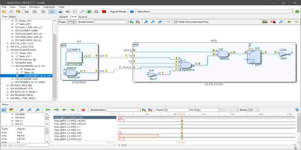
The Thin Line between Netlist and HDL

Generally, the Netlist is used to describe the different connected components inside the circuitry. It can also be used for other purposes, such as providing the nodes, instances and some of the components’ attributes.
However, it is possible for the PCB Netlist file to be considered a Hardware Description Language (HDL). In this case, it means that the Netlist has provided much more information than it is originally meant to provide.
Therefore, it can be referenced as any of the following HDLs – VHDL or Verilog. It is also possible to consider it to be a language designed for hardware compilers or input to simulators. A Netlist file example for this is the SPICE analog simulation Netlist.
Netlist File Examples, Based on the Types
You have quite a lot of options to choose from if you are choosing the Netlist files. The one you opt to go for depends on the type of connections you are looking to validate.
The following are some of the common Netlist file types:
Instance-Based vs. Net-Based
In this case, the Netlist can be clustered, based on the component instance. It could also be a net-based Netlist, which has to do with the exhaustive list of connections made to a specific network (net).
The classifications can further be broken down into the following:
- Hierarchical: in this instance, the connections are grouped into or classified, based on the layer or the physical board they are connected to.
- Flat: being flat means that all the connections are shown.
Physical vs. Logical
The Netlist can either be physical whereby the connections are physically-established or logical, which has to do with the logical optimization of the connections.
Choosing between Schematic and Netlist: What You Need to Know
Both schematic and Netlist are two different ways to feed data or information into the Printed Circuit Board (PCB).
However, the decision on which is the best tends to come up. While there may be no straight way to answering this question, we can give a few pointers/
But first, let us look at some of the similarities between the two.
Excellent Integration Options
Both the schematics and Netlists make an excellent integration for the circuit board’s layout. Thus, transferring important data into the board can be achieved with any of the two.
Design Synchronization
Integrating the PCB design also paves the way for the synchronizations to be done within the circuit board’s database. The following are synchronized:
- PCB manufacturing
- Component integration and;
- Routing options
PCB Summary
Using both the schematic and Netlist proves to be a veritable way to summarizing the structure and functionality of the design.
Inter-Generation
Netlist can be generated from the schematic and vice-versa. Ideally, you can generate either the hierarchical or flat schematics from the Netlist. Likewise, you can generate the Netlist from the schematics.
Now, let us look at some of the differences between a schematic and Netlist for a PCB:
Graphical Information
The graphical information content is often exclusive to the schematic document.
Engineer-to-Designer Communication
It is possible to use the schematic integration over the Netlist integration and it is due to the communication pathway.
With the advantages as back-annotation, cross-probing and easy-forward, the schematic integration makes it possible to the network of properties to be handed from the engineer to the designer.
Restrictions
Restrictions in this case refers to the limitations placed on the schematic or Netlist integrations. It is common with the schematic integration process, whereby the integrations must be done within the same Electronic Design Automation (EDA) software.
Formats and Availabilities
There are different formats of the Netlists, especially those require error-checking. If this is the type of Netlist you are working with, error-checking and custom editing must be done before the integration can be done on the Netlist.
The following are some of the key considerations:
- Reformatting: if the integration is to be reformatted, it has to be done with either word-processing macros or spreadsheet.
- The Netlists for the EDA software can also be reformatted.
- Ideally, the changes noticed in the process must be noticed. This helps to boost the design’s repeatability, assuming it is to be used the second.
How to Unify the PCB Schematic and Netlist
You can unify or make the schematic and PCB work like one. The following of some of the steps to actualizing this is very important.
Data Import
The first step is to capture the schematic and import the same into an initial design. Once completed, the schematic Netlist data will be used as a basis for creating the connecting lines seen in an unrouted PCB layout.
Design Consistency
The consistency of the design can be maintained only if there are no changed made to the schematic.
How to Make the Most out of the Netlist PCB File
Feeding the file into the CAM software is only one of the steps to be taken for it to be taken seriously.
For the best results, a couple of actions need to be taken. They include:
IPC-356 Netlist File Format
It is better to supply the PCB manufacturer the IPC-356 format of the Netlist file. It is a better way to manage the expectations of the Gerber files and reduce the risks of the latter from encountering errors.
Gerber Layer Placement
The reading of the IPC-356 format of Netlist file during the initial Gerber file load creates the pathway for the loading and arrangement of the Gerber layers into a logical sequence. The arrangement has to be done from top to bottom.
Layer Identification
The next step is the assignation of a type to each of the layers. This is to be followed by the following:
- Electrical definition of the layers
- Generation of the Netlist. This is to be based on the Gerber and drill data.
- The CM program then identifies the areas of different colors on the layers.
- It also follows the layer-to-layer interconnections to the plated through holes.
Discrepancies in PCB Netlist: Causes and Recommended Solutions
It is possible for differences to be spotted in the Netlist file. The following are some of the reasons for the discrepancies:
Incorrect Feature Description
The features that weren’t accurately described in the Gerber file header will only end up changing the system’s interpretation of the desired electrical path. This, in turn, often results in the inappropriate definition of the nets in the Gerber-driven referenced Netlist.
Operator Setup Errors
The discrepancies can also be caused by the mistakes by the operator. In this case, the CAM program may be forced to misunderstand the information/data before it.
Even simple errors like incorrect layer assignment can trigger erroneous raw files.
Corrupted Features
Features that are corrupt may not perform as expected. An example is the incorrect resolution of the self-intersecting polygon. This is capable of causing the system to misinterpret the data.
The best to resolve this is by using line fill instead of the polygons. You may also want to consider using the export option to export the Gerber files with the highest resolution possible – up to 2:6.
Conclusion
No matter the software you use (Altium Netlist, Allegro Netlist or Netlist KiCAD), one thing stands out – you would use the file to pursue the accurate connections of the electronic components. Talk to a professional Netlist PCB manufacturer today to guide you in the best direction to take.
