It is important to note that technological innovations aid the use of multi circuit boards. Therefore, the Multi CB works with advanced technology which makes it possible for various electronics to have multi circuit boards components.
In this interesting article, you as a designer or engineer can learn more about the PCB design and the electrical connection in different electronics. Meanwhile, the manufacturing processes for the circuit board are easy to understand. This article follows some research, reviews, and professional contributions. Also, we shall discuss about Smd components and the Smd stencils.
An Overview of the Multi CB
Over the years, the multi circuit boards are expanding in uses and applications. This is really encouraging because designers can use circuitry devices for automotive components. Also, the component library is expanding more as it gives room for versatility. Gone are the days when only limited designs are in use for consumer electronics. In fact, individual PCB can have professional design. As long as the schematic capturing device is in place, the right software is all you should consider.
The multi circuit boards have several copper traces that have proper grouping. The multi CB complexity is from varying layers as well as the interconnection links in them. Several routing methods may come from the use of several layers. It is no longer necessary to use a photo mask to design multi CB. With laser technology, schematic diagram, one can now have modern day design. The design keeps getting upgraded with more devices. The breakout board allows prototyping.
What Do Multi Circuit Boards Entail?
The multi circuit boards involve the professional methods of designing the printed circuit boards. Moreover, these include the use of appropriate designs for an electrical connection. As long as cables connect multi circuit boards in different electronics, there is need for board designers to create circuit board that can be durable.
For connections in any circuit board, the Multi CB works on thermal demands, routing, and energy distribution. Also, grounding techniques are important for any PCB design. Yearly, it is no doubt that the PCB industry is becoming more innovative with procedures for manufacturing printed circuit boards. These innovations work because of laser technology we use for these boards. Laser technology makes it possible for the testing of light which requires a simple optical amplification method.
The lasers are crucial in all electrical components of devices in use for daily activities. So, there can be emission testing of radiation in different applications involving the use of the printed circuit boards.
The Modern PCB Design Methods
In recent times, it is noteworthy that there are modern, advanced, and innovative tools designers use for PCB design. The new design tools help for easy connectivity in circuit board. Therefore, this is why the Multi CB can fit into boards irrespective of the layers.
So, you no longer have to depend on MCAD devices to connect Multi Circuit Boards. The use of the MCAD devices may rely on manual transmission for layout in the circuit board.
The printed circuit boards can now use some software in its designs. These software tools are new and can make manufacturing easier and less stressful. The PCB design can make use of flex which has some advantages. Therefore, with flex, the reliability of the board is higher. Also, the capacity is higher and automatically increases.
These days, there are numerous design softwares for your PCB design. Ultimately, you have to select software tools which the PCB industry now uses. Among these software are; Auto desk EAGLE, Altium NEXUS, Altium 365, and Ulti board.
Meanwhile, these software devices aid the manufacturing procedure for PCB. The design methods for PCB include; glossy paper step, and laser cutting method.
More on Printed Circuit Boards
The printed circuit boards are important components you find in electrical devices or electronics. The PCB makes it possible to attach electrical features in chosen areas of the circuit board. Equally, this area is possibly an outer layer of the board. Soldering is a method of affixing this component on the layers.
Additionally, the printed circuit boards have insulating layers as well as some conductive components. Consequently, the PCB makes it possible for electrical connections. Without the PCB, the electrical transmissions in our electronics will not be possible. This connection works between terminals in the board. However, this connection works in a well structured pattern which unarguably is the work of the PCB design.
There is hardly any electronics that designers and engineers don’t use printed circuit boards. Earlier, wire wraps were used in place of the PCB. Similarly, the pointed construction was in use alongside wire wraps. However, these alternatives are hardly in use for electrical connections these days.
For the circuit, it requires some designs which may need specific techniques. This helps in the laying out. However, automation may be needed for assembly. You can note that for layout of the circuit, there are new software devices engineers uses.
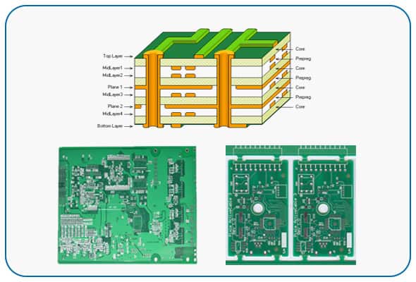
Different Layers of the Multi Printed Circuit Boards
It is important to note that for the printed circuit boards, there are various layers. Also, these layers are common but each has different features.
There is a copper layer which involves one copper. Interestingly, the one copper component has just a single side. Also, there are two layers. This implies that this circuit board has double sides. On a substrate layer, there can be two layers for each side. So, this makes it a layer with double sides. Likewise, there are multilayer boards. These circuit boards have higher density for its components. The copper traces for this kind of layer appear on the inner layer as well as the outer layer.
The Rigid-Flex PCBS
There are extensive kinds of PCB. It is important to note that each type has its unique properties. Each has its size, density, reliability, and capacity. From its name, the Rigid-Flex Printed Circuit Boards are blends of flexible with rigid boards. As a result of this combination, this kind of PCB are affixed permanently together.
This kind of circuit board is applicable in different industries. Among such industries are aerospace, military, automobiles, and telecommunications. Also, it is mostly in use to assemble electronic components. Commonly, engineers use Rigid-Flex boards in phones.
Rigid PCBs
This is another board that is different in properties from the Rigid-Flex PCBS. The design method of this board is different same as its elements for the manufacturing process. One distinguishing feature of this board is its inflexibility. Unlike flex PCB, it most likely remains impossible to bend rigid boards.
However, it is the general belief that this type of board is cheaper, more popular, and more applicable in most consumer electronics. The reason may not be far-fetched. It creates room for more space in production. As a result of being cheap, it helps designers save more.
Note that the versatility that comes with flex PCB makes it more preferable to rigid boards. It fits into different applications because designers can either fold or bend the flex PCB.
What Are Smd Stencils?

Laser technology makes it easier for the manufacturing of Smd stencils. Additionally, this often requires some precision that is high. This involves regular process quality through this high and even precision.
Interestingly, the solder paste makes the manufacturing of SMT board easier. Multi CB guarantees that Smd stencils are constantly produced with the aid of simple optical amplification method. To assemble any SMT board, engineers need the Smd stencils.
It is paramount for manufacturers to note that one of the crucial requirements of Smd stencils are the cutting precision. The cutting precision enables the assembly of the circuit board go through quality process in production.
Also, the optimal register precision is another rigorous requirement of the Smd stencils. The cutting speed often influences the amount of pads for each hour. Therefore, designers must always calculate the correct dimensions involved in manufacturing procedure of the board.
Importantly, there are some available Smd stencils for fast clipping frames. Again, the Smd stencils have calculated repeat accuracy as well as exact axial tolerance. Equally, the material for production affects the thickness level of the Smd stencils. Nowadays, the fast clipping frames are more in use as it replaces other frames such as aluminum frames.
In recent times, there are varying mounting holes used in different fast clipping frames. Furthermore, the fast clipping frames which Smd stencils have help manufacturers to save cost. It is different from the fixed frames because it saves space.
One should note that the Smd stencils are very crucial elements in the manufacturing process of SMT boards. Also, the use of the Smd stencils help to save time as it helps in saving cost. Further, the process for manufacturing is simple. It is easier to produce since one uses laser technology.
The Smd Components
There are Smd components that engineers and designers solder to boards through the use of SMT. These Smd components are available in various forms, thereby resulting in different kinds of components. To simply put, the Smd components are electronic gear that allow the direct mounting of components on surfaces of boards.
One can manufacture Smd through the SMT method. SMT simply stands for Surface Mount Technology. Arguably, it is one of the common methods of designing or producing components. The role of each Smd components helps to classify or group it. The Smd components have its identifications on boards.
Network Resistor:
This is one of the classifications of the Smd components with its identification as RA/RN. Thus, it packages many resistors using equivalent parameters in unison. Typically, the RA/RN are fitted into any digital perimeter or circuit. Similarly, its resistance identification system goes with that of chip resistor.
Chip Resistor
The chip resistor has its identification on circuit boards as R. Commonly, the resistance cost of this component is seen from the three numbers which appear on the chip resistor. Thus, this is an indication of its value.
Plus, both the first numbers and second numbers are important numbers. The third number often shows the variables of 10. R is an indication that a decimal point appears with the digits.
LED
Typically, this is a component that is grouped into two LEDs. They include the high-brightness type which mostly have colors such as yellow, white, blue, and red. These aren’t the only colors this type of LED has. Another type of LED is the ordinary one. Importantly, the LEDs polarity is measured from a particular production guideline.
IC
These kinds of Smd components have U as its identification on the PCB. Integrated Circuits, commonly referred to as IC are the most vital and most useful elements of electronic applications.
Capacitor
This has C as its identification on any circuit board. However, it has the most commonly functional ones of which MLCC is part. The material determines the division of MLCC. COG (NPO) is a division of MLCC. Also, when it comes to stability, COG (NPO) comes first. For distinction of its polarity, aluminum capacitor can be used.
Multi PCB Design Using the Appropriate Software
Earlier, we discussed that software tools help the PCB design. PCB design with the appropriate software makes the work of the designers stress-free. For the layout of printed circuit boards, specific tools are helpful. The basics of design need to be known with these tools.
Layer stack helps with the appropriate combination and blending of several images to just a simple image. These several images later become single images. To achieve this, a designer must ensure that the columns and rows of the images are the same. This implies that re-sampling is crucial when layer stack of images are in production. The multi circuit boards use techniques that make the combination work out perfectly fine.
Furthermore, it is crucial to PCB design. Thus, it deals with the arrangements of layers. This takes place in a vertical plan. Also, this arrangement of layers could be in the Z direction. However, one must be careful when the arrangements are done. Its fabrication is mostly in the form of a single idea. Therefore, the kind of board a designer uses has to be a single idea, too. Note that the single entity is the unique feature of this layer. There could be numerous options a designer can apply for stacking.
For the PCB design, an engineer needs a capture tool. This kind of tool for capturing is schematic. This schematic capturing is one of the fundamentals of your design. For the firm depiction of element symbols, schematic capturing works.
Schematic Capturing
Schematic capturing affects net connections in circuit board. Also, you find on the boards are nets. Schematic helps designers pay full attention during fabrication.
This is because it requires a lot of detailing. A schematic device helps to easily fabricate the printed circuit boards layout. The schematic tools are helpful in defining circuits. Also, it is the procedure for designing circuits in any CAD system.
While you have the CAD system, multi circuit boards can use it for pasting, cutting, and copying during fabrication. An engineer can change any paper design using schematic capturing to representations that are electronic. Schematic capturing is useful for the arrangements of elements into any schematic sheets. Thus, it finally helps in fabricating all designs that can be electrically transmitted. And this helps in producing the physical layout.
Component Library
When designing the high degree printed circuit boards, multi CB uses some component library. The component library is an integral system of any design. One advantage with it is the minimal decrease in hazard or exposure to alterations among varying products.
The component library also helps in board connectivity. The features of the library make design simple for designers. This library helps for quick extension of components. Also, it comes with patterns that are accessible and common to design.
Thus, the component library helps in quick acceleration during fabrication. It aids smooth synergy among designers, engineers, and developers. One advantage with component library is how it helps to simplify every code logically. You can also reuse your component library anytime. It is not rigid because it gives room for testability.
Component library is becoming more common among different fields. It aids quicker UI development and are not monolithic. It comes with clear and fast ways to use. One thing with the library is that it can resist bugs as long as its development centers around testing. The library is the fusion of varying components to serve the same purpose.
Routing Features
For the design, there are routing features that developers can use. These features go with the printed circuit boards layout. The routing always comes with steps in designing circuits. It gradually mounts on some earlier steps known as placements. Importantly, this often indicates the spot for every operating component of the printed circuit boards.
Signaling standard affects the routing method one uses during manufacturing. This also affects routing topology. The traces are important for the connection in the PCB. They join elements which are the internal layers. Note that there are the high speed as well as low speed standards.
Furthermore, multi circuit boards require that one gets the appropriate MCAD verification. This verification is integral because it indicates how every circuit board connect rightly. Mechanical verification if not properly carried out can poorly affect the circuit boards. If you are new to design, it is expedient to study carefully how multi CB work on connections for boards.
An engineer’s ECAD device can come with MCAD kit. If it is so, it makes design interesting. In fact, it is always regarded as the perfect combination when the ECAD device has the MCAD kit. With this, it is faster to carve various board segment. Thus, an engineer can authenticate the mechanical pressure from it.
The Multi CB Layout And Fabrication in One Application
It is possible that the multi circuit boards have the PCB layout and fabrication all embedded in a single application. It becomes attainable when you use the appropriate software tools. The importance of these software devices can never be overemphasized.
This is because one can have challenges when fabricating PCB design. However, the design software comes with simple application. The application covers every verification you need to carry out. There are other applications that group these devices to various forms. It could be stressful as a result of splitting it. To make design simpler, the PCB design, fabrication, and layout can be in just one group. Note that, it is an advanced form of workflow. The accuracy of one’s design needs verification. With this, you can easily do that without any delay.
While you are preparing for your design, you need to check out for design rules. No doubt, the MCAD kit and ECAD device help one’s new design get proper fabrication. Detailing for every board involves some drafts as well as assembly illustrations.
When you intend to import each design, your MCAD kit serves as a significant tool. It is designed in such a way that enables developers, engineers, and designers get the support needed for transitioning. You can convert from ECAD device without any stress to MCAD kit because they work interchangeably. During your design process, a good MCAD kit helps with the arrangements of the boards.
Conclusion
One needs accuracy when it comes to designing PCB. Multi circuit boards use modern day tools to facilitate fabrication. It is important for an engineer or designer to use a component library as it contains the right elements for manufacturing.
The PCB design requires some precision. The Smd stencils are important for manufacturing SMT boards. We discussed elaborately on what the Smd stencils are. Also, the transitioning from ECAD device to MCAD kit is effortless, although the MCAD may rely on manual application.
The software tools come with simple applications. The layer stack on its own has to do with the arrangements of layers. So, we can say that it is important for our printed circuit boards. Get the right tools to aid your PCB design.
