PCB filters are an essential component in electronic circuitry. They are used to remove unwanted noise and interference from the signal, ensuring that the circuit operates smoothly. Altium is a popular software tool used for designing PCB filters.
Altium offers a range of features for designing PCB filters. It has a user-friendly interface that makes it easy to create and edit designs. The software also has a wide range of tools for analyzing and testing the filter design, ensuring that it meets the required specifications.
Designing PCB filters can be a complex process, but with Altium, it is made easy. The software provides a range of templates and libraries that can be used to design filters quickly and efficiently. Additionally, Altium has a large community of users who share their knowledge and expertise, making it easy to find solutions to any design problems that may arise.
What is a PCB Filter?
A PCB filter is an electronic component that is designed to remove unwanted signals or noise from a printed circuit board (PCB) and ensure that the signal quality is maintained. It is a critical component in any electronic circuit, as it helps to reduce the impact of electromagnetic interference (EMI) and radio frequency interference (RFI), which can cause a variety of problems, including signal distortion and data loss.
There are different types of PCB filters, including low-pass filters, high-pass filters, band-pass filters, and band-stop filters. Each type of filter has a specific frequency range that it is designed to operate within, and it can be used to filter out unwanted signals that fall outside of this range.
PCB filters can be implemented using a variety of different technologies, including passive components such as resistors, capacitors, and inductors, as well as active components such as operational amplifiers (op-amps) and transistors. The choice of technology will depend on the specific requirements of the circuit and the desired level of performance.
In summary, a PCB filter is an essential component in any electronic circuit that helps to ensure signal quality by removing unwanted noise and interference. Different types of filters are available depending on the specific requirements of the circuit, and they can be implemented using a variety of different technologies to achieve the desired level of performance.
Designing a PCB Filter in Altium
Creating a New PCB Project
To design a PCB filter in Altium, start by creating a new PCB project. In Altium, click on File > New > Project, and select PCB Project. Give your project a name and select a location to save it. Once you have created a new project, you can start designing your schematic.
Schematic Design
In the schematic design phase, you will create a circuit diagram of the filter. To create a new schematic, click on File > New > Schematic. Altium provides a wide range of schematic symbols and components that you can use to design your circuit. You can also create custom symbols and components if the ones provided do not meet your requirements. Once you have designed your schematic, you can move on to the PCB layout design phase.
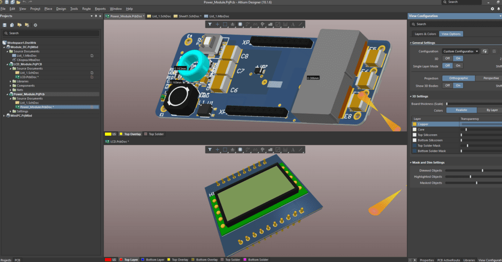
PCB Layout Design
In the PCB layout design phase, you will transfer your schematic design to the PCB layout. To create a new PCB layout, click on File > New > PCB. Altium provides a range of tools and features to help you design your PCB layout, such as Design Rules Check (DRC), 3D visualization, and more. You can also use the built-in autorouting feature to automatically route your PCB traces. Once you have completed your PCB layout design, you can move on to generating Gerber files.
Generating Gerber Files
Gerber files are the standard format used to manufacture PCBs. To generate Gerber files in Altium, click on File > Fabrication Outputs > Gerber Files. Altium will generate a set of Gerber files that you can send to your PCB manufacturer to manufacture your PCB.
In conclusion, designing a PCB filter in Altium involves creating a new PCB project, designing a schematic, designing a PCB layout, and generating Gerber files. Altium provides a range of tools and features to help you design your PCB filter, and once you have completed the design, you can generate Gerber files and send them to your PCB manufacturer for production.
Testing and Verification
Simulating the PCB Filter Design
Before prototyping and testing the PCB filter design, it is essential to simulate the design using an Electronic Design Automation (EDA) software such as Altium Designer. The simulation helps to verify the design’s performance, identify any potential issues, and optimize the design for better performance.
Simulating the PCB filter design involves setting up the simulation environment by defining the input and output signals, component models, and simulation parameters. The simulation results are then analyzed to determine the filter’s frequency response, gain, and other performance parameters.
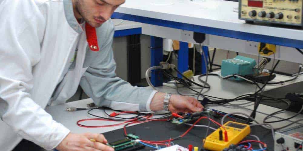
Prototyping and Testing
Once the simulation results are satisfactory, the next step is to prototype and test the PCB filter design. Prototyping involves creating a physical version of the design using the appropriate components, PCB layout, and manufacturing techniques.
Testing the PCB filter design involves measuring its performance using test equipment such as a network analyzer, oscilloscope, and signal generator. The testing process helps to verify the design’s performance, identify any issues, and optimize the design for better performance.
During the testing process, it is essential to ensure that the PCB filter design meets the required specifications such as the frequency response, insertion loss, and return loss. Any issues identified during testing should be addressed by modifying the design and repeating the simulation and testing process.
In conclusion, testing and verification are crucial steps in the PCB filter design process. Simulating the design using an EDA software and prototyping and testing the physical design helps to ensure that the design meets the required specifications and performs as expected.
Common Issues and Troubleshooting

When working with PCB filters in Altium, there are a few common issues that you may encounter. Here are some troubleshooting tips to help you resolve these issues:
Issue 1: Incorrect Filter Response
One common issue with PCB filters is an incorrect filter response. This can be caused by a variety of factors, such as incorrect component values, incorrect filter topology, or incorrect layout. To troubleshoot this issue, you can try the following:
- Check the component values to ensure they match the filter design.
- Verify that the filter topology is correct for the desired response.
- Check the layout to ensure that the components are placed correctly and that there are no routing issues.
Issue 2: Noise and Interference
Another common issue with PCB filters is noise and interference. This can be caused by a variety of factors, such as poor grounding, incorrect component values, or incorrect filter topology. To troubleshoot this issue, you can try the following:
- Verify that the grounding is correct and that there are no ground loops.
- Check the component values to ensure they match the filter design.
- Verify that the filter topology is correct for the desired response.
Issue 3: EMI and EMC Compliance
EMI and EMC compliance is an important consideration when designing PCB filters. If your filter is not EMI and EMC compliant, it can cause interference with other devices and may not meet regulatory requirements. To troubleshoot this issue, you can try the following:
- Verify that the filter design meets the relevant EMI and EMC standards.
- Check the layout to ensure that there are no routing issues that could cause EMI or EMC problems.
- Use simulation tools to verify that the filter meets the desired EMI and EMC performance.
By following these troubleshooting tips, you can resolve common issues with PCB filters in Altium and ensure that your designs meet the desired performance requirements.
Conclusion

In conclusion, PCB filters are a crucial component in any electronic system that requires noise reduction. Altium is a popular software tool that can be used to design and simulate these filters.
Through the use of Altium, designers can easily create and test various filter topologies to find the optimal design for their specific application. The software’s simulation capabilities allow designers to see how the filter will perform in real-world scenarios, ensuring that the final design meets the required specifications.
When designing PCB filters in Altium, it is important to consider factors such as the filter’s frequency response, insertion loss, and group delay. These parameters can be adjusted and optimized to achieve the desired performance characteristics.
Overall, Altium is a powerful tool for designing and simulating PCB filters. Its user-friendly interface and simulation capabilities make it an ideal choice for designers looking to create high-performance filters for their electronic systems.
