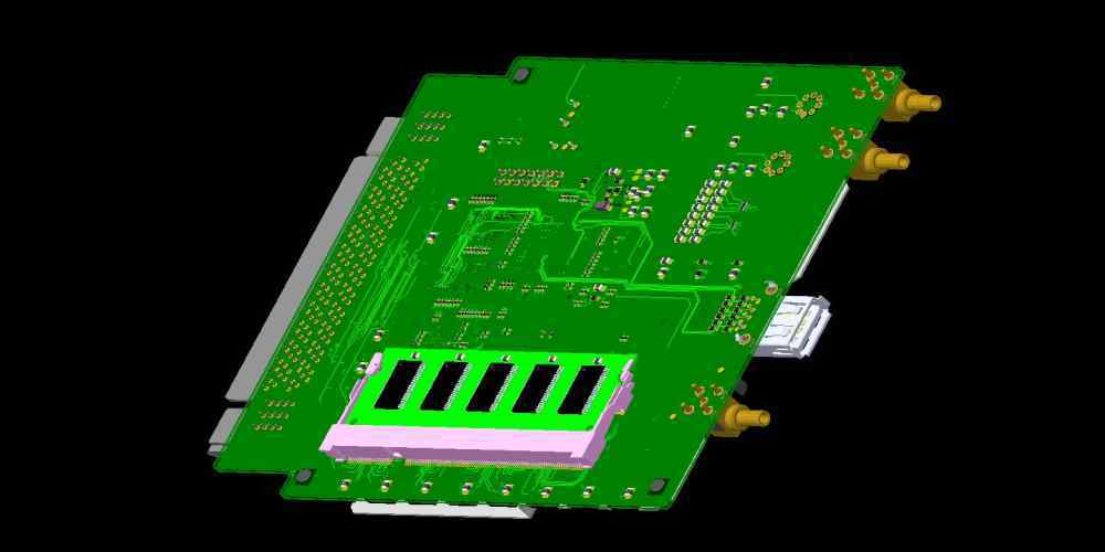
PCB layout Gerber is a crucial aspect of printed circuit board design. It is the file format used to transfer the design data from the PCB layout software to the manufacturer. The Gerber file contains all the necessary information such as the copper traces, drill holes, and other design elements that need to be printed onto the board.
The Gerber file format has been in use for over 50 years and has become the industry standard for PCB manufacturing. It allows for accurate and precise reproduction of the PCB design, ensuring that the final product meets the requirements of the designer. The Gerber file format also allows for easy communication between the designer and the manufacturer, as it provides a clear and concise representation of the design.
What is PCB Layout Gerber?
PCB Layout Gerber is a file format that contains all of the information necessary to create a printed circuit board (PCB). It includes information about the placement of components, the routing of traces, and the location of holes and cutouts. The Gerber format is the industry standard for PCB manufacturing and is supported by most PCB design software.
The Gerber format is a vector format, which means that it uses mathematical equations to describe the shapes and patterns on the PCB. This makes it easy to scale the design up or down to fit different PCB sizes. It also means that the Gerber format is very precise and accurate, which is important for ensuring that the PCB is manufactured correctly.
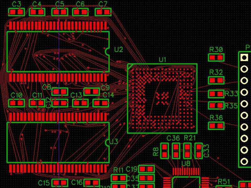
The Gerber format is typically used to create the artwork for each layer of the PCB. This includes the top and bottom copper layers, the silk screen layer, and the solder mask layer. Each layer is created as a separate Gerber file, which is then combined with the other layers to create the final PCB design.
In summary, PCB Layout Gerber is a file format that contains all of the information necessary to create a PCB. It is a vector format that is precise and accurate, and is used to create the artwork for each layer of the PCB.
Why is PCB Layout Gerber Important?
PCB layout Gerber is a crucial aspect of the PCB manufacturing process. It is a set of files that contain all the information required to manufacture the PCB. The Gerber file format is the standard format used by PCB manufacturers worldwide.
The PCB layout Gerber includes information about the board layers, copper traces, pads, vias, and other components. The Gerber files are used by PCB manufacturers to create the PCB layout on the actual board. The files are used to create the PCB design on a computer, which is then transferred to the PCB manufacturing equipment.
The importance of PCB layout Gerber cannot be overstated. It ensures that the PCB design is accurate and precise. Any errors in the Gerber files can lead to manufacturing defects, which can cause the PCB to malfunction or fail entirely.
Furthermore, the Gerber files are used to create a stencil for the solder paste. The stencil is used to apply the solder paste to the PCB, which is necessary for the placement of the components. Any errors in the Gerber files can lead to misalignment of the components, which can cause the PCB to malfunction or fail.
In conclusion, the PCB layout Gerber is a critical aspect of the PCB manufacturing process. It ensures that the PCB design is accurate and precise, which is essential for the proper functioning of the PCB. Any errors in the Gerber files can lead to manufacturing defects, which can cause the PCB to malfunction or fail entirely.
How to Create a PCB Layout Gerber File

When it comes to creating a printed circuit board (PCB), the layout is an essential step in the process. A PCB layout Gerber file is a standard file format that provides the manufacturer with the necessary information to create the PCB. Here are the basic steps to create a PCB layout Gerber file.
Step 1: Design the PCB Layout
First, design the PCB layout using a software tool such as Eagle, KiCAD, or Altium Designer. The software tool should have the ability to generate Gerber files. Ensure that the design is complete and error-free before proceeding to the next step.
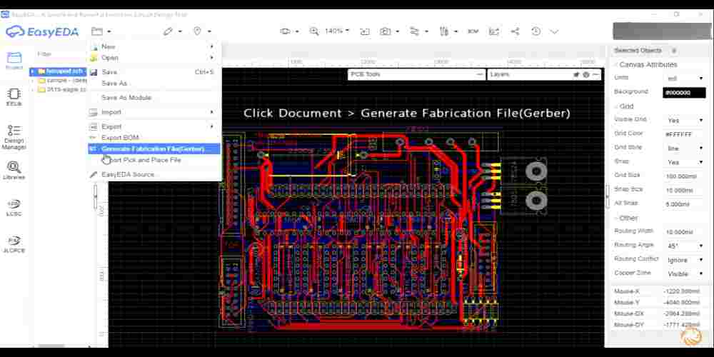
Step 2: Generate the Gerber Files
Next, generate the Gerber files using the software tool. The Gerber files should include all the necessary layers, such as the copper layers, solder mask, and silkscreen. Ensure that the file naming convention is correct and that all the layers are included in the file.
Step 3: Check the Gerber Files
Before submitting the Gerber files to the manufacturer, it is essential to check them for any errors. Use a Gerber viewer tool to view the files and ensure that all the layers are aligned correctly. Check for any missing or extra layers and make sure that the file naming convention is correct.
Step 4: Submit the Gerber Files
Once the Gerber files are error-free, submit them to the manufacturer for production. Ensure that the manufacturer understands the file naming convention and the layer order. It is also important to provide any other necessary information, such as the board thickness, copper weight, and drill sizes.
In conclusion, creating a PCB layout Gerber file is a crucial step in the PCB manufacturing process. By following these steps, you can ensure that the Gerber files are error-free and ready for production.
Best Practices for Creating a PCB Layout Gerber File
Creating a PCB layout Gerber file is a crucial step in the manufacturing process of a printed circuit board. A well-designed Gerber file ensures that the board is manufactured accurately and efficiently. Here are some best practices to follow when creating a PCB layout Gerber file:
1. Use a Standard Naming Convention
It’s essential to use a standard naming convention when naming your Gerber file. This helps to avoid confusion and ensures that the manufacturer can easily identify the different layers of the PCB. A standard naming convention typically includes a two-letter code followed by a number. For example, the top layer might be named “TP1.”
2. Include a Readme File
Including a readme file with your Gerber file is a good practice. The readme file should include information about the PCB design, such as the number of layers, materials used, and any special instructions for manufacturing. This information helps the manufacturer to understand the design and ensures that the board is manufactured accurately.
3. Check for Errors
Before submitting your Gerber file, it’s essential to check for errors. Common errors include missing or incorrect drill holes, missing or incorrect board outline, and missing or incorrect copper traces. Using a Gerber viewer to check your file is a good practice. This ensures that the manufacturer receives a file that is free of errors and can manufacture the board accurately.
4. Use a Standard Format
Using a standard format for your Gerber file is crucial. The most common format is the RS-274X format, which is widely used in the industry. Using a standard format ensures that the manufacturer can easily read and interpret the file and ensures that the board is manufactured accurately.
Following these best practices ensures that your PCB layout Gerber file is accurate, efficient, and easy to manufacture.
Common Mistakes When Creating a PCB Layout Gerber File
When creating a PCB layout Gerber file, there are several common mistakes that can be made. Here are a few of the most frequent mistakes and how to avoid them:
1. Not Checking for Design Rule Errors
One of the most common mistakes when creating a PCB layout Gerber file is not checking for design rule errors. Design rule errors can cause a variety of problems, such as shorts, opens, and incorrect spacing. To avoid this mistake, it’s important to check for design rule errors before generating the Gerber file.
2. Not Including All Necessary Layers
Another common mistake is not including all necessary layers in the Gerber file. This can result in missing components or incorrect placement of components. To avoid this mistake, make sure to include all necessary layers, such as the top and bottom copper layers, silkscreen layers, and drill layers.
3. Not Setting the Correct Units
Setting the incorrect units is another common mistake when creating a PCB layout Gerber file. This can result in incorrect dimensions and spacing. To avoid this mistake, make sure to set the correct units before generating the Gerber file.
4. Not Checking for Overlapping Objects
Not checking for overlapping objects is another common mistake when creating a PCB layout Gerber file. Overlapping objects can cause shorts and other problems. To avoid this mistake, it’s important to check for overlapping objects before generating the Gerber file.
5. Not Converting Fonts to Outlines
Finally, not converting fonts to outlines is another common mistake when creating a PCB layout Gerber file. If fonts are not converted to outlines, they may not appear correctly in the final product. To avoid this mistake, make sure to convert all fonts to outlines before generating the Gerber file.
By avoiding these common mistakes, you can ensure that your PCB layout Gerber file is accurate and free of errors.
Tools for Viewing and Editing PCB Layout Gerber Files
When it comes to viewing and editing PCB layout Gerber files, there are several tools available in the market. These tools are designed to help PCB designers and manufacturers to view and edit the Gerber files accurately and efficiently. Here are some of the most popular tools that you can use:
1. Gerber Viewers
Gerber viewers are software tools that are specifically designed to view Gerber files. These tools allow you to view the different layers of the PCB design, including the copper layers, silkscreen layers, and solder mask layers. Some of the popular Gerber viewers include:
- Gerbv
- ViewMate
- GC-Prevue
2. PCB Design Tools
Most of the PCB design tools available in the market also come with a built-in Gerber viewer. These tools allow you to view and edit the Gerber files within the software itself. Some of the popular PCB design tools that come with a built-in Gerber viewer include:
- Altium Designer
- Eagle PCB
- KiCAD
3. Gerber Editors
Gerber editors are software tools that allow you to edit the Gerber files directly. These tools are useful when you need to make minor changes to the PCB design, such as adjusting the size of the pads or changing the thickness of the traces. Some of the popular Gerber editors include:
- CAM350
- DipTrace
- Pentalogix
In conclusion, choosing the right tool for viewing and editing PCB layout Gerber files depends on your specific needs. Whether you need a simple Gerber viewer or a comprehensive PCB design tool with a built-in Gerber viewer, there are plenty of options available in the market.
Conclusion
In conclusion, PCB layout gerber is a crucial aspect of the PCB design process. It involves converting the design files into a format that can be used by the manufacturer to produce the actual PCB. The gerber files contain all the necessary information about the copper traces, pads, vias, and other components on the board.
One of the most important aspects of PCB layout gerber is ensuring that the design meets the manufacturer’s specifications. This includes factors such as the minimum trace width, minimum clearance, and drill sizes. Failure to adhere to these specifications can result in manufacturing defects, which can be costly to correct.
It is also important to ensure that the gerber files are accurate and error-free. This can be achieved through the use of design rule checks (DRCs) and other software tools. Additionally, it is crucial to carefully review the gerber files before sending them to the manufacturer to ensure that they are correct.
Overall, PCB layout gerber is a complex process that requires careful attention to detail and a thorough understanding of the manufacturing process. By following best practices and adhering to manufacturer specifications, designers can ensure that their PCBs are produced correctly and with minimal defects.
