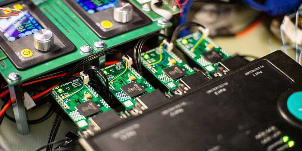
The process of manufacturing printed circuit boards or PCB assemblies is very complex. This process involves several stages. However, the most crucial stages are design, build, and test. When developing a new board, the first stage is usually prototyping. This stage often involves various iterative steps such as design, build, test that usually end up with achieving a production quality design.
The process is quite similar however, the board design goes through some continuous change in this case. Sometimes, the design stage will require you to convert schematic to PCB design layout. However, there are some cases where you aren’t required to do that.
Is a Schematic really needed for your PCB Design?
The answer to this question will lead to answering more questions since this is a broad question. Therefore, we have decided to answer some questions below.
What is a PCB schematic?
A PCB schematic refers to the graphical description of the components and how they are interconnected for a successful electrical circuit design.
What does a PCB schematic comprise?
A schematic features labels and symbols. These labels and symbols are crucial elements that help in defining or illustrating the functionality of the circuit board design. This usually comprises both active and passive components, ground connections, terminals, reference indicators, nodes, connectors, and nets.
How do you integrate a PCB to Schematic converter?
You can see schematics as canvases used for making electrical circuit designs. In this case, the PCB designer is creates, reviews, and evaluates the design to be sure all rules pertaining to connectivity are well adhered to before the schematic is converted to a PCB design layout that will be produced later.
The answers to these questions have revealed some crucial details about schematics. With these answers, one can conclude that the schematic is the starting point when creating a new electrical circuit design. Most times, the designer draws the schematic as a template for the printed circuit board layout.
When designing a PCB assembly, you might not need a schematic since the design process is so simple. In most cases it is crucial to create a schematic first in order to confirm electrical functionality and as well save time as regards the board layout design. Also, this is important as the complexity of most PCB designs determines the successful creation of a schematic.
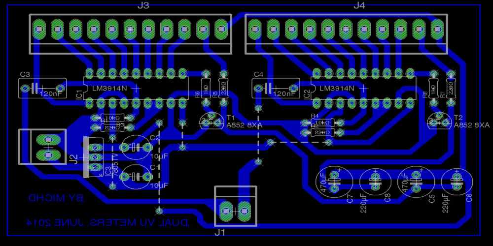
Designing Your Board Layout
Before, the development of PCB design software, PCB designers drew PCB layouts and schematics by hand. Those who were skilled at doing this were sought after. However, things have changed now as technology has made life much easier. Drawing schematics and PCB layout by hand was time consuming and required a lot of effort. Today, there are a wide range of ECAD tools that help designers simplify the creation of schematics and PCB layouts.
Also, when you need convert schematic to PCB design layout, there is now an auto concatenation process. PCB to schematic converter PCB design software can help you achieve this successfully. However, there are certain steps involved in this design process. Below are steps you need to follow in order to prepare your design for manufacturing.
PCB Layout Steps
Select a board size
The majority of ECAD tools come with default board sizes. These board sizes have different area and thicknesses you can select. It is much advisable to check with your contract manufacturer before you select your board size. This is because some board sizes may have too much waste which will end up adding to your manufacturing costs.
Create the stackup
You will need to define the types of layers, board materials, and the number of layers in this step.
Arrange components
After creating the stackup, the next step is the placement of components on the printed circuit board. In this step, the PCB designer must ensure all spacing and clearance rules are strictly adhered to. This will help you achieve a successful PCB design.
Route the traces
The most challenging step in a PCB layout is trace routing. This is even more challenging when working with multilayer boards that have many vias–plated through holes (PTHs) that vertically transmit signals from internal signal and ground planes. During trace routing, ensure you adhere to proper spacing and clearance.
Check for errors
Errors could occur during PCB layout and as such, you need to be sure of the PCB layout you are sending off for manufacturing. Checking for errors include carrying out a DRC analysis. A DRC analysis helps you know if your design adheres to the design rules and constraints. You need to be sure these rules were set based on the DFM guidelines of your contract manufacturer to enable manufacturability.
The steps above are crucial for creating a PCB layout. PCB assembly design is a complex process and as such there is a level of time needed to achieve a manufacturable design. The type of ECAD tool you use will determine how easy it is to convert schematic to PCB design layout.
Tools to Convert Schematic to PCB Design

There are various applications for electronics and printed circuit boards. PCBs have found their use in various industries. Therefore, it isn’t surprising that there a wide range of PCBA design packages. However, there is a variation when it comes to the functionality and capabilities PCB design software programs can offer.
Therefore, you need the review the capabilities of the program before you choose any ECAD program. Some software feature a PCB to schematic converter. There are some critical problems you need to take into consideration. These issues include:
Useful PCBA Capabilities
Component library
It can be a daunting task to create landing pattern and schematic symbols for your circuit board layout. You need to make use of your online component library if your PCB design software has no extensive component library. This will prevent you from generating component libraries manually.
Netlist verification
Netlist verification is known to be an important capability for schematic creation. This helps you check if all the wiring is properly connected. Improper connections can result in floating nodes, shorts, and opens.
Auto component placement
Auto component placement is another important function which lays out the circuit board according to component type. These functions’ effectiveness varies across tools. However, it usually offers a good starting point and as such adheres to clearance rules and spacing.
Autorouting
When there are many vias in a PCB design, auto routing can be a more helpful option than component placement especially. However, there is a need to make changes, particularly to ensure practices for good signal integrity design. Convert PCB to Schematic
Bilateral concatenation between schematic and PCB layout
While all circuit board design software packages feature unilateral concatenation, not all packages feature bilateral concatenation. Software packages with this feature can update the schematic according to changes made to the layout.
Tips to Consider When you need to Convert Schematic to PCB Layout
Check for some features in your PCB editor
When designing a circuit board, the first stage is a PCB layout. Since, the design process is usually carried out by your software. You need to check your software for the necessary features you need. Your PCB project will determine the features you need. Check for features like break, route, via, SMD, polygon, and break.
Select the ideal board size
When schematics are converted to board layout, the components on the schematic will occupy a side. You need to place the components on your board and check for any free space. If there is a free space, you can use your software to shrink the board size.
Check signals to know routing
The quality of a circuit board will depend on signal paths. Any mess with the signal can affect the routing. Signals are capable of taking various paths. Also, it is possible to design a circuit board with straight paths. The application of your circuit board will determine the type of signal path you need. In most cases, you will need to combine curved and straight designs.
Make sure you clean the PCB layout
Make sure you check your PCB design thoroughly before finalizing it. Check the traces to ensure they are neat enough to enjoy improved clearance. Also, you can check if everything in the layout fits well. You can as well check your components and connections.
Ensure you run DRC
The DRC check is one of the most important step in PCB layout. It helps you to check if your design meets up with the design rules. The design rule check helps in determining compliance with the design rule.
Gerber to Schematic Converter
Some PCB design software come with the Gerber to schematic converter. The process of converting Gerber to schematic requires following some steps. Gerber files do not have any information as regards components. Therefore, without a BOM or schematic from the initial design, you cannot convert a Gerber into a schematic
Also, It is impossible to reverse engineer a Gerber file back into a circuit board in some software packages. You can only achieve this by reverse engineering the Gerber using another software and then import the circuit board in another software.
It is possible to recreate the schematic if you have a schematic or a BOM. If the BOM and schematic is available, then it is much easier to design the schematic and convert to a circuit board.
Circuit Diagram to PCB Layout Converter Online
There are several software packages that offer circuit diagram to PCB layout converter online. Before you learn how to convert a circuit diagram to a PCB layout, you need to understand what a circuit diagram is. This circuit diagram has to do with the visual representation for electrical circuit by integrating symbols or basic images of parts.
A circuit diagram has hundreds of symbols. These include images of components like a resistor or a battery or symbols for components like inductors and capacitors. Altium designer, OrCAD, and kiCAD are examples of circuit diagram to PCB layout converter online. So, how do you convert a circuit diagram to a PCB layout.
Prepare to synchronize your PCB design
Ensure you review your circuit diagram to get prepared for the layout. Check for duplicated circuitry such as forgotten parts or copies. Now, you need to ensure everything is carefully checked. This process requires compiling the schematic that will produce all internal information of the design.
Import design data to a circuit board
The next step is to convert the circuit diagram or schematic to a PCB layout. To do this, you need a circuit board to transfer to. For instance, in Altium designer, you will transfer the Design data from the circuit diagram to PCB design. Altium has a PCB editor and the schematic editor in the same program. Also, it features a circuit diagram to PCB layout converter online command in its main menu.
Define the layer stack
There are some tasks you should carry out before you commence with the layout. Here, it is crucial to gather your necessary information and confirm with suppliers. Also, you will need to configure the circuit board for the board layers stackup.
What to Consider when Designing a PCB Schematics
A schematic features labels and symbols. These labels and symbols are crucial elements that help in defining or illustrating the functionality of the circuit board design. This usually comprises both active and passive components, ground connections, terminals, reference indicators, nodes, connectors, and nets.
When designing a PCB assembly, you might not need a schematic since the design process is so simple. In most cases it is crucial to create a schematic first in order to confirm electrical functionality and as well save time as regards the board layout design. Also, this is important as the complexity of most PCB designs determines the successful creation of a schematic.
Conclusion
Before, the development of PCB design software, PCB designers drew PCB layouts and schematics by hand. Those who were skilled at doing this were sought after. However, things have changed now as technology has made life much easier. Drawing schematics and PCB layout by hand was time consuming and required a lot of effort. Today, there are a wide range of ECAD tools that help designers simplify the creation of schematics and PCB layouts.
