Schematic to circuit board is a process that involves converting an electronic schematic into a physical circuit board. This process is essential in the design and production of electronic devices, ranging from simple toys to complex medical equipment. The schematic is the blueprint of the electronic circuit, and the circuit board is the physical representation of the schematic.
The process of converting a schematic to a circuit board involves several steps. First, the schematic is designed using specialized software. The software allows the designer to create a visual representation of the electronic circuit, including the components and their connections. Once the schematic is complete, the software generates a netlist, which is a list of all the connections between the components. The netlist is then used to create the physical circuit board using computer-aided design (CAD) software. The CAD software generates a layout of the circuit board, including the placement of the components and the routing of the connections. Finally, the physical circuit board is manufactured using specialized equipment and materials.

Schematic Design
Creating the Schematic
The first step in designing a circuit board is creating the schematic, which is a graphical representation of the circuit’s components and their connections. It is important to choose a software tool that is intuitive and easy to use to create the schematic. Some popular tools include Altium Designer, Eagle PCB, and KiCAD.
When creating the schematic, it is important to consider the functionality of the circuit and the components that will be used. It is also important to follow industry standards and guidelines to ensure that the circuit will perform as expected and meet safety requirements.
Schematic Review and Validation
After the schematic is created, it is important to review and validate it to ensure that it is accurate and will work as intended. This involves checking the schematic for errors, such as incorrect connections or missing components.
One way to validate the schematic is to use a simulation tool to test the functionality of the circuit. This can help identify any potential issues before the circuit is built.
It is also important to review the schematic with other members of the design team to get feedback and ensure that everyone is on the same page. This can help catch any errors or issues that may have been overlooked.
Overall, the schematic design process is a critical step in designing a circuit board, and it is important to take the time to create an accurate and validated schematic to ensure the success of the project.
PCB Layout Design
Creating the PCB Layout
After the schematic design is complete, it’s time to create the PCB layout. This involves placing the components on the board and routing the traces that connect them. The PCB layout design is critical to the success of the circuit, as it affects the electrical performance, manufacturability, and reliability of the final product.
To create a PCB layout, you can use a PCB design software tool such as Altium Designer, Eagle PCB, or KiCAD. These tools allow you to import the schematic design and then place the components on the board. You can also define the board size, shape, and layers, as well as set up design rules for trace width, spacing, and clearance.
When placing the components, you should consider their size, orientation, and spacing. You should also group them logically based on their functions and connections. You can use the software’s auto-placement feature to speed up the process, but you should also manually adjust the placement to optimize the layout.
PCB Design Review and Validation
Once you have created the PCB layout, you should review and validate it to ensure that it meets the design requirements and specifications. This involves checking the electrical connectivity, signal integrity, power distribution, thermal management, and mechanical constraints of the board.
You can use the software’s design rule check (DRC) feature to detect any errors or violations in the layout. You should also simulate the circuit using a SPICE tool or a signal integrity analyzer to verify its performance. You can use the software’s 3D visualization feature to inspect the board from different angles and perspectives.
After you have reviewed and validated the PCB layout, you can generate the manufacturing files such as Gerber files, drill files, and bill of materials (BOM). You should also prepare the documentation such as assembly drawings, test procedures, and user manuals.
In conclusion, the PCB layout design is a crucial step in the process of converting a schematic into a circuit board. By following the best practices and guidelines, you can create a layout that is optimized for performance, manufacturability, and reliability.
Prototype and Testing

Fabrication and Assembly
Once the schematic has been finalized, the next step is to create a physical prototype of the circuit board. This involves fabricating the board and assembling the components onto it.
The fabrication process typically involves using a software program to generate the necessary files for a manufacturer to produce the board. This includes the copper traces, drill holes, and any other necessary markings or features. The manufacturer will then produce the board using a process such as etching or milling.
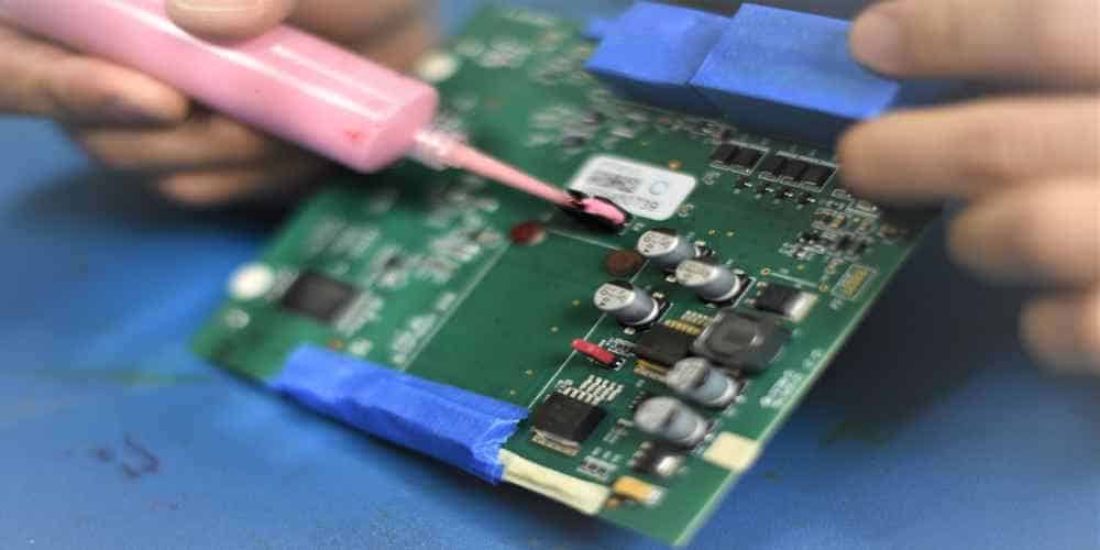
Once the board has been fabricated, the components can be assembled onto it. This involves placing the components onto the board and soldering them in place. It is important to follow the schematic and ensure that each component is placed in the correct location and orientation.
Testing and Troubleshooting
After the board has been assembled, it is time to test the circuit. This involves applying power to the board and measuring the output of each component. It is important to test each component individually to ensure that it is functioning correctly.
If any issues are found during testing, the troubleshooting process begins. This involves identifying the source of the problem and making any necessary changes to the circuit or components. This may involve re-soldering a component, replacing a faulty component, or making changes to the schematic.
Overall, the prototype and testing phase is a crucial step in the circuit board design process. It allows for any issues to be identified and corrected before the final product is produced.
Production and Manufacturing
Gerber File Generation
The first step in producing a circuit board from a schematic is to generate Gerber files. Gerber files are a set of instructions that tell the PCB manufacturer how to create the board. They include information such as the location of components, the size of the board, and the placement of vias and traces.
Generating Gerber files is a critical step in the manufacturing process. If the files are not generated correctly, the PCB manufacturer will not be able to produce a functional board. Therefore, it is important to double-check the files before sending them to the manufacturer.
PCB Manufacturing
Once the Gerber files have been generated, the PCB manufacturer can begin the manufacturing process. The first step is to print the circuit board onto a copper-clad board. This is done using a process called photo-etching, which involves exposing the board to UV light and then etching away the unwanted copper.
After the board has been printed, it is drilled to create holes for the components. The holes are then plated with copper to create vias, which allow the components to be connected to each other.
Finally, the board is coated with a layer of solder mask and a layer of silkscreen. The solder mask protects the board from damage during soldering, while the silkscreen provides labeling and other information about the board.
Assembly
Once the PCB has been manufactured, it is time to assemble the components. This is done using a process called surface mount technology (SMT), which involves placing the components onto the board and then soldering them in place.
SMT is a highly automated process that allows for fast and accurate assembly of components. However, it requires specialized equipment and expertise. Therefore, it is often outsourced to a third-party assembly house.
In conclusion, the production and manufacturing of a circuit board from a schematic involves several critical steps, including Gerber file generation, PCB manufacturing, and assembly. Each step requires careful attention to detail to ensure that the final product is functional and reliable.
