A universal PCB, also known as a prototype PCB is a circuit board used in the design stage for testing out ideas and for the verification of system concepts. This universal PCB is important in the manufacture of new PCB-compatible devices and machines.
They are so crucial in helping manufacturers perfect the function of the PCBs before going into large-scale production, to avoid a waste of resources and time. Another important use of a prototype PCB is the manufacture of single electronic device units.
Most are made from glass fiber as opposed to phenolic paper which gives off a brown color associated with those brown circuit boards. This is because glass fiber is more durable, and as such, more economic. Some manufacturers typically have their circuit board holes tinned to forestall oxidation and make soldering easier.
Most universal printed circuit boards are suited to soldering components, but others have spring terminals, but these are more for hobbyists than for complex design. These circuit boards are readily available for your test projects and are a cart buy away on most related websites. You just have to make sure that you know the difference between the variants in the market and that you select the one that is specific to your needs.
Description
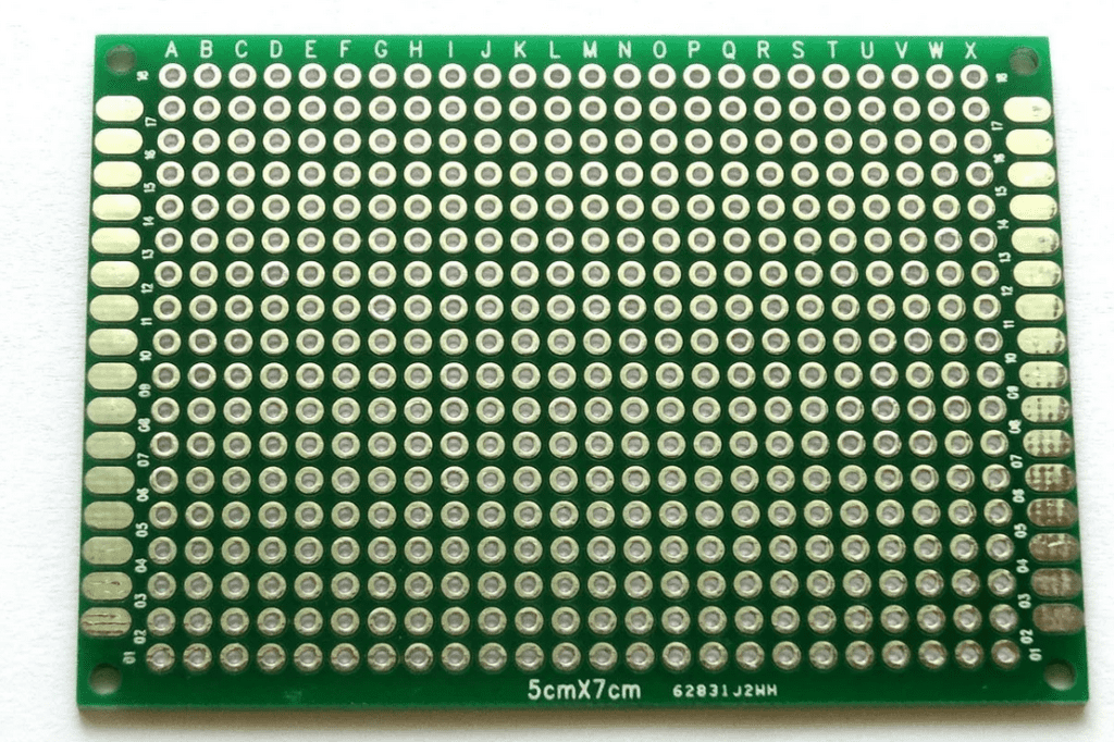
Universal circuit boards are of different shapes, sizes, and designs. from big circuit boards with sides that are several dozen centimeters long to rectangular PCBs that are almost the size of a postage stamp.
PCBs in the shape of euro cards with edge connectors and spherical PCBs, which are intended for LED lighting and computer card prototype, respectively, are also available. They are available in single-sided and double-sided varieties and are constructed from glass-epoxy laminates and paper laminates with varying thicknesses, ranging from 0.7 to 1.6 mm.
Despite the variation in the market, universal PCBs have an unspoken industry standard for dimensions that most universal PCBs use. If you’re purchasing on websites, the boards usually come in a group of between five to ten pieces, each piece having an approximate 5 by 7 cm dimension, and is usually double-sided. The thickness is usually 1.6mm. Each grid is about 2.5 mm long and each hole diameter is approximately 1mm.
For all the good universal circuit boards are known for, because they are a prototype, the conversation still comes back to printed circuit boards when one considers large-scale production of a working and tested PCB idea. The case may not always lead to large-scale production.
The project at hand may be small-scale involving singular units. However, most electronic projects that would involve a universal PCB for prototyping tend toward the end of large-scale production.
Hence the use of universal PCBs is more temporary in this way and the use of more generally known printed circuit boards is more permanent. So let’s discuss printed circuit boards and how they bring out the beauty of prototyping.
Printed Circuit Boards

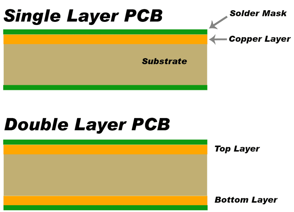
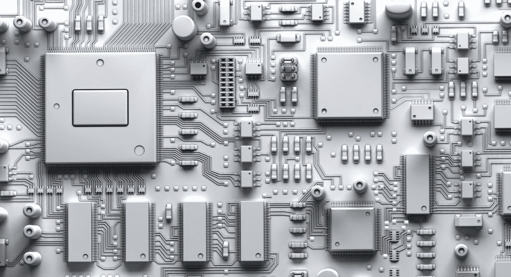
When connecting electronic components securely, electrical engineers utilize printed circuits or printed wire boards. It has layers that are laminated together and are both conductive and insulating.
To create a pattern of traces, planes, and other characteristics that are used in the manufacturing of each of the conductive layers, one or more copper sheet layers may be laminated onto or sandwiched between sheet layers of a non-conductive substrate. This may be done either on top of or between the sheet layers of the substrate. On a level surface, these characteristics have a pattern that looks like a wire mesh.
Conductive pads on the board’s outer layers are used to connect electrical components to it. Usually, the geometry of these conductive pads is intended to mimic the terminals of the electrical component. Nowadays, practically every electrical device uses this board, therefore production is higher than it has ever been, albeit automated.
This board would need a ridiculous amount of extra work to physically construct because the circuit layout would need to be extremely precise. Printed circuit boards are created using a method known as electronic design automation, which prevents the waste of human labor and establishes a uniform standard.
Electronic systems like integrated circuits and printed circuit boards are created using a method based on a collection of software tools. These instruments are used by chip designers to develop and evaluate semiconductor chips.
Given that some current chips can have up to a billion microcomponents working as one, this automation approach considerably decreases the possibility of error that may result from manual design.
What are the 3 Types of Printed Circuit Boards?
One-sided Printed Circuit Board
This one-sided printed circuit board has a single layer of substrate or base material. A tiny layer of metal, typically copper since it is an effective electrical conductor, is applied to the substrate’s one end. The final silkscreen coat may be put to the top to indicate components of the board after a protective solder mask is typically set on the peak of the copper layer.
On only one side of this PCB, there are numerous circuits and electronic parts. For simple circuits, this form of the module works best, and beginners frequently design and construct this kind of board first.
Two-sided Printed Circuit Board
Comparatively speaking, this kind of PCB is far more common than single-sided boards. The substrate of the board has metal conductive layers on both sides, and elements are attached to both sides as well. The PCB has holes that allow circuitry on one side to connect to circuits on the other.
Through-hole or surface mount technology was employed to connect the circuits on each side of this type of circuit board. In through-hole technology, leads are thin wires that are fed through the holes and soldered to the appropriate component at each end. In contrast to through-hole technology, surface mount technology does not use wires. In its stead, several tiny leads are soldered directly to the board.
Multilayer PCBs
These PCBs include additional layers above and beyond the top and bottom layers found in a double-sided structure, increasing the density and complexity of PCB designs. Multilayer printed circuit boards (PCBs) enable designers to create extremely thick and complex designs because they have access to numerous layers in these configurations.
Power planes, which are employed as additional layers in this design, reduce the amounts of electromagnetic interference that are emitted by designs while also supplying the circuit supply with power.
Signal levels are positioned in the center of power planes to reduce EMI levels. Before any of these circuit boards can be used after design, and a confirmation of the schematics, they have to be printed.
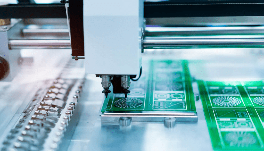
PCB Printing
The material and tools used to create a circuit board can vary significantly depending on the type of etching used for PCB fabrication. However, whether etching is done mechanically, with machine assistance, or with an etching solution, there is a standard set of tools that can be used, which includes a PC and printer.
Photosensitive PCB boards, transparent slides, Indian ink, cotton buds, paper towel, UV light source, NaOH, sodium persulfate, two bottles made of plastic or glass, rubber gloves, Drill bits, two empty 1L bottles, copper boards, a laser printer, fine sandpaper or a kitchen scrubber, acetone, hydrogen peroxide, acetone, thinner, hydrochloric acid, and kitchen cleaner are some of the materials you’ll need.
Printing can follow certain various techniques depending on some factors. Those techniques are:
Acid etching: this method requires a lot of safety precautions, is a little slow, and uses a variety of materials, including the etchant. The quality of the PCB you get will vary depending on the materials you select, but generally speaking, it is a good method for circuits with low to medium degrees of complexity.
Circuits with smaller cables and closer wiring frequently employ other methods. The UV etching process uses more expensive ingredients, some of which might not be commonly available, to transfer your PCB layout onto your PCB board. The processes, however, are fairly simple and can lead to finer and more complex circuit layouts.
Routing method: For this method to be used, specialist equipment that can mechanically remove superfluous copper from the board or run empty separators between wires is required. It can be expensive to buy one of those pieces of equipment and renting one usually necessitates access to a nearby workshop. However, this method works great if you need to routinely duplicate the circuit and produce high-quality PCBs.
Large production companies often use the laser etching process, but other institutions could also have access to it. The concept is similar to mechanical etching, however, LASER beams are used to etch the board. The PCB layout for your circuit is what comes next.
You must use an etchant-resistant material to sketch the circuits before acid etching. You may easily get specialized markers if you want to draw by hand. For medium-sized to big circuits, this is inappropriate.
However, the substance that is used the most frequently is the ink for laser printers. This is frequently done by converting your circuit’s schematic design into a PCB layout utilizing PCB layout software. For developing and generating PCB layouts, a variety of open-source software is available.
Once you are satisfied with the schematic for the PCB design on your computer, you should check that the circuit board and the paper are the right sizes by comparing the size of the design in the software to theirs.
To print the diagram, use the software’s File menu. It should be printed on glossy paper similar to magazine paper. Make sure the circuit is mirrored before attempting that. This is a printing option available in the majority of PCB design layout programs. After printing, take care not to touch the area of the paper that has ink on it because it might get on your hands.
Iron the Printed PCB Layout
Orient the circuit board and the paper circuit schematic. The copper portion of the circuit board should be with the schematic facing it. Your iron should be on at this point. Set the iron to the cotton setting and wait for it to heat up.
Before placing it lightly on top of the paper covering the circuit board, the iron needs to be warmed up. For 30 to 45 seconds, the iron should remain in place. Lift the iron, place it aside with care, and then transport the circuit board to the nearest water source. The paper ought to be affixed to the circuit board; avoid removing it.
As the water starts to flow, hold the circuit board down. The paper should start to fall off gradually and completely after that. If some areas seem particularly difficult to complete, you might try soaking a little longer.
If everything went as planned, you ought to have a copper board with your signal traces and PCB pads etched out in black toner. drying a board. The huge water droplets can simply be dripped out or gently wiped off using a napkin or sponge. A maximum of 30 seconds should be used, and excessive rubbing of the circuit may cause the ink to peel off.
Etch the Board
Etch the board with acid. The copper thickness on the board is therefore eliminated by the etching solution, leaving only the wiring for the final circuit. Select an etching agent. A common choice for an etchant is ferric chloride. However, different chemical solutions or ammonium persulfate crystals can be employed.
Other etching techniques, particularly the mechanical and laser printer techniques, etch the board using machines and laser beams and are more suited for intricate circuitry. Prepare the acid etchant.
Depending on the acid etch you choose, there can be additional instructions. For instance, although other etchants can be employed right away, some crystalline acids must first be dissolved in hot water.
Put the board completely in the acid. Every three to five minutes, remember to stir the mixture. Remove the board and wash it after any additional copper has been etched off of it. Get rid of the utilized drawing substance for insulation.
Specialized solvents are available for almost all insulating drawing materials used in PCB layout drawings. If none of these are available to you, you can still use fine sandpaper. The description above up till this point defines how PCBs are printed. Once they are printed, they can be used in a wide range of fields.
Common Uses of PCBs
Medical Devices
As technology develops and reveals new capabilities, the healthcare industry uses PCBs in increasing amounts. PCBs are utilized in a variety of devices, including those used for monitoring, therapy, and diagnosis.
In many instances, especially when used for implantation, PCBs in this field have to adhere to high sanitary regulations. In addition, boards for many other uses, such as monitors for ERs, must be quite tiny. HDI is therefore widely utilized in medical PCBs for devices like:
Medical imaging equipment: PCBs are frequently used in ultrasonic scanners as well as in the computers that gather and evaluate the images they produce.
Monitors: To provide reliable results, electronic components are needed for devices like patients’ heart rate, blood pressure, and blood glucose monitors, among others.
Infusion pumps: these pumps, like insulin and analgesia pumps controlled by patients, provide a patient with precisely measured amounts of fluid. PCBs, contribute to the accuracy and dependability of these items’ performance.
Devices used internally: Small PCBs are necessary for the operation of pacemakers and other internal devices.
More and more applications for electronics are being developed in the medical field. PCBs will become more crucial to healthcare as technology advances and smaller, denser, more dependable boards are made possible.
Consumer Electronics
A wide range of other consumer products relies on PCBs to function. PCBs are becoming more common in our daily lives as electronics are being incorporated into more products. Manufacturers are producing smaller smartphones and laptops with better capabilities, necessitating small PCBs with a high volume of connections.
PCBs used in consumer electronics must also be relatively low-cost to keep the final product price low. Manufacturers also want dependable boards because they rely on their products to perform as expected to stay in business.
PCBs are found in a wide range of consumer products, including smartphones, tablets, smartwatches, radios, and other communications devices all require PCBs to function. PCBs are used in both personal and commercial computers.
PCBs are used in entertainment systems such as televisions, stereos, and video game consoles. fridges, microwaves, and coffee machines, for example, contain electronic components and PCBs.
The use of PCBs in consumer products shows no signs of abating. The percentage of Americans who own a smartphone has risen to 77 percent and is continuing to rise. Any devices that were not previously electronic are now gaining advanced electronic functionality.
Industrial Equipment
Electronic components power much of the equipment in manufacturing and distribution centers, as well as other types of industrial facilities. To withstand the harsh conditions found in industrial facilities, PCBs used in the industrial sector must frequently be extremely powerful and long-lasting.
When PCBs are used in industry, it is imperative that the material is protected from abrasion, vibration, high temperatures, and harsh chemicals. In order to fulfill this requirement for durability, industrial printed circuit boards (PCBs) may be thicker than other types of PCBs and constructed out of materials that can withstand high temperatures. Through-hole technology may be incorporated into industrial PCB assembly services in order to boost the boards’ durability.
Manufacturing electric drills and presses are powered by PCB-based electronics. PCBs are found in components that power a wide range of industrial equipment. This category of power equipment includes solar power cogeneration equipment, DC-to-AC power inverters, and other items.
PCBs are commonly used in the powering of equipment that measures and controls pressure, temperature, and other variables. As robotics, industrial IoT technology, and other types of advanced technology become more common, new industrial applications for PCBs emerge. The following industrial applications make use of PCBs.
Automobile Industry
Automobiles are increasingly incorporating electronic components. Previously used only for windshield wipers and headlight switches, PCBs now enable many advanced features that make driving safer and easier.
A PCB may need to withstand high temperatures or vibrations depending on the application. If they are used in a car safety feature, it is also critical that they work consistently. To address these issues, manufacturers may employ aluminum or copper substrates, or high-temperature laminates, and through-hole mounted components. Because of their vibration resistance, they also use flex-rigid PCBs. PCBs are in automotive devices listed below.
Stereos and systems: they integrate navigation and entertainment and rely on printed circuit boards (PCBs).
Control systems: Many of the systems that control the car’s basic functions rely on electronics powered by PCBs. Engine management systems and fuel regulators are examples of these.
Sensors: As automobiles become more advanced, manufacturers incorporate an increasing number of sensors. These sensors can detect blind spots and warn drivers of potential hazards. PCBs are also required for systems that allow cars to parallel park automatically.
These sensors are part of what makes self-driving cars possible. Because fully autonomous vehicles are expected to become more common in the future, a large number of printed circuit boards are being used.
The use of PCBs in all these fields started with design and testing and involved universal PCBs at some point. So while printed circuit boards are celebrated and are all the craze of the electronics industry, universal PCBs are the real heroes, being involved in research and general efforts that push the boundary of electrical and electronic development.
